


2N5655, 2N5657
Plastic NPN Silicon
High−Voltage Power
Transistor
These devices are designed for use in line−operated equipment such
as audio output amplifiers; low−current, high−voltage converters; and http://onsemi.com AC line relays.
Features
0.5 AMPERE
• Excellent DC Current Gain −
hFE = 30−250 @ IC = 100 mAdc |
|
|
|
|
|||
• Current−Gain − Bandwidth Product − |
|
|
|
|
|||
fT = 10 MHz (Min) @ IC = 50 mAdc |
|
|
|
||||
• Pb−Free Packages are Available* |
|
|
|
|
|
|
|
MAXIMUM RATINGS (Note 1) |
|
|
|
|
|
|
|
|
|
|
|
|
|
|
|
Rating |
|
Symbol |
|
2N5655 |
|
2N5657 |
Unit |
|
|
|
|
|
|
|
|
Collector−Emitter Voltage |
|
VCEO |
|
250 |
|
350 |
Vdc |
Collector−Base Voltage |
|
VCB |
|
275 |
|
375 |
Vdc |
Emitter−Base Voltage |
|
VEB |
|
6.0 |
Vdc |
||
Collector Current − Continuous |
|
IC |
|
0.5 |
Adc |
||
Peak |
|
|
|
1.0 |
|
||
|
|
|
|
|
|
||
Base Current |
|
IB |
|
1.0 |
Adc |
||
Total Device Dissipation @ TC = 25°C |
|
PD |
|
|
20 |
W |
|
Derate above 25°C |
|
|
|
0.16 |
W/°C |
||
|
|
|
|
|
|
||
Operating and Storage Junction |
|
TJ, Tstg |
|
– 65 to +150 |
°C/W |
||
Temperature Range |
|
|
|
|
|
|
|
|
|
|
|
|
|
|
|
THERMAL CHARACTERISTICS |
|
|
|
|
|
|
|
|
|
|
|
||||
Characteristic |
|
Symbol |
|
Max |
Unit |
||
|
|
|
|
|
|
||
Thermal Resistance, |
|
qJC |
|
6.25 |
°C/W |
||
Junction−to−Case |
|
|
|
|
|
|
|
|
|
|
|
|
|
|
|
Stresses exceeding Maximum Ratings may damage the device. Maximum
Ratings are stress ratings only. Functional operation above the Recommended Operating Conditions is not implied. Extended exposure to stresses above the Recommended Operating Conditions may affect device reliability.
1. Indicates JEDEC registered data.
*For additional information on our Pb−Free strategy and soldering details, please download the ON Semiconductor Soldering and Mounting Techniques Reference Manual, SOLDERRM/D.
POWER TRANSISTORS
NPN SILICON
250−350 VOLTS, 20 WATTS
TO−225AA
CASE 77−09
STYLE 1
MARKING DIAGRAM
YWW 2
N565xG
Y |
= Year |
|
||
WW |
= Work Week |
|||
2N565x = Device Code |
||||
|
|
x = 5 or 7 |
|
|
G |
= Pb−Free Package |
|||
|
|
|
||
ORDERING INFORMATION |
||||
|
|
|
|
|
Device |
|
Package |
|
Shipping |
|
|
|
|
|
2N5655 |
|
TO−225 |
|
500 Units / Bulk |
|
|
|
|
|
2N5655G |
|
TO−225 |
|
500 Units / Bulk |
|
|
(Pb−Free) |
|
|
|
|
|
|
|
2N5657 |
|
TO−225 |
|
500 Units / Bulk |
|
|
|
|
|
2N5657G |
|
TO−225 |
|
500 Units / Bulk |
|
|
(Pb−Free) |
|
|
|
|
|
|
|
♥ Semiconductor Components Industries, LLC, 2006 |
1 |
Publication Order Number: |
October, 2006 − Rev. 9 |
|
2N5655/D |
2N5655, 2N5657
ELECTRICAL CHARACTERISTICS (TC = 25_C unless otherwise noted) (Note 2)
Characteristic |
|
Symbol |
Min |
Max |
Unit |
|
|
|
|
|
|
|
|
OFF CHARACTERISTICS |
|
|
|
|
|
|
|
|
|
|
|
|
|
Collector−Emitter Sustaining Voltage |
2N5655 |
VCEO(sus) |
250 |
− |
Vdc |
|
(IC = 100 mAdc (inductive), L = 50 mH) |
2N5657 |
|
350 |
− |
|
|
Collector−Emitter Breakdown Voltage |
2N5655 |
V(BR)CEO |
250 |
− |
Vdc |
|
(IC = 1.0 mAdc, IB = 0) |
2N5657 |
|
350 |
− |
|
|
Collector Cutoff Current |
|
ICEO |
|
|
mAdc |
|
(VCE = 150 Vdc, IB = 0) |
2N5655 |
|
− |
0.1 |
|
|
(VCE = 250 Vdc, IB = 0) |
2N5657 |
|
− |
0.1 |
|
|
Collector Cutoff Current |
|
ICEX |
|
|
mAdc |
|
(VCE = 250 Vdc, VEB(off) = 1.5 Vdc) |
2N5655 |
|
− |
0.1 |
|
|
(VCE = 350 Vdc, VEB(off) = 1.5 Vdc) |
2N5657 |
|
− |
0.1 |
|
|
(VCE = 150 Vdc, VEB(off) = 1.5 Vdc, TC = 100_C) |
2N5655 |
|
− |
1.0 |
|
|
(VCE = 250 Vdc, VEB(off) = 1.5 Vdc, TC = 100_C) |
2N5657 |
|
− |
1.0 |
|
|
Collector Cutoff Current |
|
ICBO |
|
|
mAdc |
|
(VCB = 275 Vdc, IE = 0) |
2N5655 |
|
− |
10 |
|
|
(VCB = 375 Vdc, IE = 0) |
2N5657 |
|
− |
10 |
|
|
Emitter Cutoff Current (VEB = 6.0 Vdc, IC = 0) |
|
IEBO |
− |
10 |
mAdc |
|
ON CHARACTERISTICS |
|
|
|
|
|
|
|
|
|
|
|
|
|
DC Current Gain (Note 3) |
|
hFE |
|
|
− |
|
(IC = 50 mAdc, VCE = 10 Vdc) |
|
|
25 |
− |
|
|
(IC = 100 mAdc, VCE = 10 Vdc) |
|
|
30 |
250 |
|
|
(IC = 250 mAdc, VCE = 10 Vdc) |
|
|
15 |
− |
|
|
(IC = 500 mAdc, VCE = 10 Vdc) |
|
|
5.0 |
− |
|
|
Collector−Emitter Saturation Voltage (Note 3) |
|
VCE(sat) |
|
|
Vdc |
|
(IC = 100 mAdc, IB = 10 mAdc) |
|
|
− |
1.0 |
|
|
(IC = 250 mAdc, IB = 25 mAdc) |
|
|
− |
2.5 |
|
|
(IC = 500 mAdc, IB = 100 mAdc) |
|
|
− |
10 |
|
|
Base−Emitter Voltage (IC = 100 mAdc, VCE = 10 Vdc) (Note 3) |
|
VBE |
− |
1.0 |
Vdc |
|
DYNAMIC CHARACTERISTICS |
|
|
|
|
|
|
|
|
|
|
|
|
|
Current−Gain − Bandwidth Product (IC = 50 mAdc, VCE = 10 Vdc, f = 10 MHz) (Note 4) |
fT |
10 |
− |
MHz |
|
|
Output Capacitance (VCB = 10 Vdc, IE = 0, f = 100 kHz) |
|
Cob |
− |
25 |
pF |
|
Small−Signal Current Gain (IC = 100 mAdc, VCE = 10 Vdc, f = 1.0 kHz) |
|
hfe |
20 |
− |
− |
|
2.Indicates JEDEC registered data for 2N5655 Series.
3.Pulse Test: Pulse Width v 300 ms, Duty Cycle v 2.0%.
4.fT is defined as the frequency at which |hfe| extrapolates to unity.
(WATTS) |
40 |
|
|
|
|
|
|
|
|
|
|
|
|
|
|
|
|
|
|
|
|
|
|
||
30 |
|
|
|
|
|
|
|
|
|
|
|
|
|
|
|
|
|
|
|
|
|
|
|
||
|
|
|
|
|
|
|
|
|
|
|
||
|
|
|
|
|
|
|
|
|
|
|
|
|
DISSIPATION |
20 |
|
|
|
|
|
|
|
|
|
|
|
|
|
|
|
|
|
|
|
|
|
|
||
|
|
|
|
|
|
|
|
|
|
|
||
|
|
|
|
|
|
|
|
|
|
|
|
|
, POWER |
10 |
|
|
|
|
|
|
|
|
|
|
|
|
|
|
|
|
|
|
|
|
|
|
||
|
|
|
|
|
|
|
|
|
|
|
||
|
|
|
|
|
|
|
|
|
|
|
|
|
D |
|
|
|
|
|
|
|
|
|
|
|
|
P |
0 |
|
|
|
|
|
|
|
|
|
|
|
|
|
|
|
|
|
|
|
|
|
|
|
|
|
|
|
|
|
|
|
|
|
|
|
|
|
|
25 |
50 |
75 |
100 |
125 |
150 |
||||||
TC, CASE TEMPERATURE (°C)
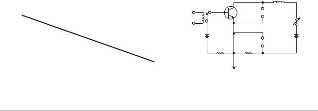
|
|
50 mH |
|
X |
|
|
|
200 |
Hg RELAY |
TO SCOPE |
|
+ |
|
+ |
6.0 V |
|
50 V |
|
Y |
− |
|
|
|
300 |
1.0 |
|
Figure 1. Power Derating |
Figure 2. Sustaining Voltage Test Circuit |
Safe Area Limits are indicated by Figures 3 and 4. Both limits are applicable and must be observed.
http://onsemi.com
2
 Loading...