


 Loading...
Z80 Family
CPU User Manual
User Manual
80
=L/2* :RUOGZLGH +HDGTXDUWHUV ‡ ( +DPLOWRQ $YHQXH ‡ &DPSEHOO &$
7HOHSKRQH ‡ )D[ ‡ ZZZ =L/2* FRP

= &38 8VHU¶V 0DQXDO
This publication is subject to replacement by a later edition. To determine whether a later edition exists, or to request copies of publications, contact:
ZiLOG Worldwide Headquarters
910 E. Hamilton Avenue Campbell, CA 95008 Telephone: 408.558.8500 Fax: 408.558.8300 www.ZiLOG.com
Document Disclaimer
ZiLOG is a registered trademark of ZiLOG Inc. in the United States and in other countries. All other products and/or service names mentioned herein may be trademarks of the companies with which they are associated.
©2001 by ZiLOG, Inc. All rights reserved. Information in this publication concerning the devices, applications, or technology described is intended to suggest possible uses and may be superseded. ZiLOG, INC. DOES NOT ASSUME LIABILITY FOR OR PROVIDE A REPRESENTATION OF ACCURACY OF THE INFORMATION, DEVICES, OR TECHNOLOGY DESCRIBED IN THIS DOCUMENT. ZiLOG ALSO DOES NOT ASSUME LIABILITY FOR INTELLECTUAL PROPERTY INFRINGEMENT RELATED IN ANY MANNER TO USE OF INFORMATION, DEVICES, OR TECHNOLOGY DESCRIBED HEREIN OR OTHERWISE. Except with the express written approval of ZiLOG, use of information, devices, or technology as critical components of life support systems is not authorized. No licenses are conveyed, implicitly or otherwise, by this document under any intellectual property rights.
80

= &38 8VHU¶V 0DQXDO
LLL
Table of Contents
2YHUYLHZ
$UFKLWHFWXUH
&38 5HJLVWHUV $ULWKPHWLF /RJLF 8QLW$/8 ,QVWUXFWLRQ 5HJLVWHU DQG &38 &RQWURO
3LQ 'HVFULSWLRQ
2YHUYLHZ 3LQ )XQFWLRQV
7LPLQJ
2YHUYLHZ ,QVWUXFWLRQ )HWFK
0HPRU\ 5HDG 2U :ULWH
,QSXW RU 2XWSXW &\FOHV %XV 5HTXHVW$FNQRZOHGJH &\FOH ,QWHUUXSW 5HTXHVW$FNQRZOHGJH &\FOH 1RQ 0DVNDEOH ,QWHUUXSW 5HVSRQVH
+$/7 ([LW
3RZHU 'RZQ$FNQRZOHGJH &\FOH
3RZHU 'RZQ 5HOHDVH &\FOH
,QWHUUXSW 5HVSRQVH
2YHUYLHZ
,QWHUUXSW (QDEOH 'LVDEOH &38 5HVSRQVH
+DUGZDUH DQG 6RIWZDUH ,PSOHPHQWDWLRQ ([DPSOHV
+DUGZDUH
0LQLPXP 6\VWHP $GGLQJ 5$0
0HPRU\ 6SHHG &RQWURO
80 |
7DEOH RI &RQWHQWV |

= &38 8VHU¶V 0DQXDO
LY
,QWHUIDFLQJ '\QDPLF 0HPRULHV
6RIWZDUH ,PSOHPHQWDWLRQ ([DPSOHV
2YHUYLHZ RI 6RIWZDUH )HDWXUHV ([DPSOHV RI 6SHFLILF = ,QVWUXFWLRQV
([DPSOHV RI 3URJUDPPLQJ 7DVNV
= &38 ,QVWUXFWLRQ 'HVFULSWLRQ
2YHUYLHZ
,QVWUXFWLRQ 7\SHV $GGUHVVLQJ 0RGHV ,QVWUXFWLRQ 2S &RGHV
= ,QVWUXFWLRQ 6HW
=$VVHPEO\ /DQJXDJH = 6WDWXV ,QGLFDWRU )ODJV $GG 6XEWUDFW )ODJ
= ,QVWUXFWLRQ 'HVFULSWLRQ
%LW /RDG *URXS
%LW /RDG *URXS
([FKDQJH %ORFN 7UDQVIHU DQG 6HDUFK *URXS
%LW$ULWKPHWLF *URXS
*HQHUDO 3XUSRVH$ULWKPHWLF DQG &38 &RQWURO *URXSV
%LW$ULWKPHWLF *URXS
5RWDWH DQG 6KLIW *URXS
%LW 6HW 5HVHW DQG 7HVW *URXS
-XPS *URXS
&DOO$QG 5HWXUQ *URXS
,QSXW DQG 2XWSXW *URXS
7DEOH RI &RQWHQWV |
80 |

< %27 7UGT U /CPWCN
X
List of Instructions
$'&$V
$'& +/ VV
$''$+/
$''$,; G
$''$,< G
$''$Q $''$U
$'' +/ VV
$'' ,; SS
$'' ,< UU $1' V
%,7 E +/
%,7 E ,; G
%,7 E ,< G
%,7 E U &$// FF QQ
&&) &3 V
&3' &3'5
&3,
&3,5
&3/
'$$
'(& ,;
'(& ,<
'(& P
'(& VV
',
'-1= H
80 |
/LVW RI ,QVWUXFWLRQV |

< %27 7UGT U /CPWCN
XK
(,
(; 63 +/
(; 63 ,;
(; 63 ,<
(;$)$)
(; '( +/
(;;
+$/7
,0
,0
,0
,1$Q
,1 U &
,1& +/
,1& ,; G
,1& ,< G
,1& ,;
,1& ,<
,1& U
,1& VV
,1'
,1'5
,1,
,1,5
-3 +/
-3 ,;
-3 ,<
-3 FF QQ
-3 QQ
-5 1& H
-5 & H
-5 H
-5 1= H
-5 = H
/LVW RI ,QVWUXFWLRQV |
80 |

< %27 7UGT U /CPWCN
XKK
/' %&$
/' '($
/' +/ Q
/' +/ U /' ,; G Q
/' ,; G U /' ,< G Q
/' ,< G U /' QQ$
/' QQ GG
/' QQ +/
/' QQ ,;
/' QQ ,<
/'$%&
/'$'(
/'$, /'$5
/' GG QQ
/' GG QQ
/' ,$
/' ,; QQ /' ,< QQ
/' U +/
/' U ,; G
/' U ,< G /' 5$
/' U U
/' U Q /' 63 +/
/' 63 ,;
80 |
/LVW RI ,QVWUXFWLRQV |

< %27 7UGT U /CPWCN
XKKK
/' 63 ,<
/''
/''5
/',
/',5
1(*
123
25 V
27'5
27,5
287 & U
287 Q$
287'
287,
323 ,;
323 ,<
323 TT
386+ ,;
386+ ,<
386+ TT
5(6 E P
5(7
5(7 FF
5(7,
5(71
5/ P
5/$
5/& +/
5/& ,; G
5/& ,< G
5/& U
5/&$
5/'
55 P
/LVW RI ,QVWUXFWLRQV |
80 |

< %27 7UGT U /CPWCN
KZ
55$
55& P
55&$
55'
567 S
6%&$V
6%& +/ VV
6&)
6(7 E +/
6(7 E ,; G
6(7 E ,< G
6(7 E U
6/$P 65$P
65/ P
68% V
;25 V
80 |
/LVW RI ,QVWUXFWLRQV |

< %27 7UGT U /CPWCN
Z
/LVW RI ,QVWUXFWLRQV |
80 |
< %27 7UGT U /CPWCN
ZK
List of Figures
)LJXUH = &38 %ORFN 'LDJUDP
)LJXUH = &38 5HJLVWHU &RQILJXUDWLRQ
)LJXUH = , 2 3LQ &RQILJXUDWLRQ
)LJXUH %DVLF &38 7LPLQJ ([DPSOH
)LJXUH ,QVWUXFWLRQ 2S &RGH )HWFK
)LJXUH 0HPRU\ 5HDG RU :ULWH &\FOH
)LJXUH ,QSXW RU 2XWSXW &\FOHV
)LJXUH %XV 5HTXHVW$FNQRZOHGJH &\FOH
)LJXUH ,QWHUUXSW 5HTXHVW$FNQRZOHGJH &\FOH
)LJXUH 1RQ 0DVNDEOH ,QWHUUXSW 5HTXHVW 2SHUDWLRQ
)LJXUH +$/7 ([LW )LJXUH 3RZHU 'RZQ$FNQRZOHGJH
)LJXUH 3RZHU 'RZQ 5HOHDVH &\FOH 1R
)LJXUH 3RZHU 'RZQ 5HOHDVH &\FOH 1R
)LJXUH 3RZHU 'RZQ 5HOHDVH &\FOH 1R
)LJXUH 0RGH ,QWHUUXSW 5HVSRQVH 0RGH
)LJXUH 0LQLPXP = &RPSXWHU 6\VWHP )LJXUH 520 DQG 5$0 ,PSOHPHQWDWLRQ )LJXUH$GGLQJ 2QH :DLW 6WDWH WR DQ 0 &\FOH )LJXUH$GGLQJ 2QH :DLW 6WDWH WR$Q\ 0HPRU\ &\FOH
)LJXUH ,QWHUIDFLQJ '\QDPLF 5$0V
)LJXUH 6KLIWLQJ RI %&' 'LJLWV %\WHV
80 |
/LVW RI )LJXUHV |

< %27 7UGT U /CPWCN
ZKK
/LVW RI )LJXUHV |
80 |

< %27 7UGT U /CPWCN
ZKKK
List of Tables
7DEOH ,QWHUUXSW (QDEOH 'LVDEOH )OLS )ORSV
7DEOH %XEEOH /LVWLQJ
7DEOH 0XOWLSO\ /LVWLQJ
7DEOH +H[ %LQDU\ 'HFLPDO &RQYHUVLRQ 7DEOH 7DEOH %LW /RDG *URXS /'
7DEOH %LW /RDG *URXS /' 386+ DQG 323
7DEOH ([FKDQJHV (; DQG (;; 7DEOH %ORFN 7UDQVIHU *URXS
7DEOH %ORFN 6HDUFK *URXS 7DEOH %LW$ULWKPHWLF DQG /RJLF 7DEOH *HQHUDO 3XUSRVH$) 2SHUDWLRQ
7DEOH %LW$ULWKPHWLF 7DEOH 5RWDWHV DQG 6KLIWV
7DEOH %LW 0DQLSXODWLRQ *URXS 7DEOH-XPS &DOO DQG 5HWXUQ *URXS
7DEOH 5HVWDUW *URXS
7DEOH ,QSXW *URXS 7DEOH %LW$ULWKPHWLF DQG /RJLF 7DEOH 0LVFHOODQHRXV &38 &RQWURO
80 |
/LVW RI 7DEOHV |

< %27 7UGT U /CPWCN
ZKX
/LVW RI 7DEOHV |
80 |

= &38 8VHU¶V 0DQXDO
[Y
0DQXDO 2EMHFWLYHV
This user manual describes the architecture and instruction set of the Z80 CPU.
$ERXW 7KLV 0DQXDO
ZiLOG recommends that the user read and understand everything in this manual before setting up and using the product. However, we recognize that users have different styles of learning: some will want to set up and use their new evaluation kit while they read about it; others will open these pages only to check on a particular specification. Therefore, we have designed this manual to be used either as a how to procedural manual or a reference guide to important data.
,QWHQGHG $XGLHQFH
This document is written for ZiLOG customers who are experienced at working with microprocessors or in writing assembly code or compilers.
0DQXDO 2UJDQL]DWLRQ
The Z80 CPU User’s Manual is divided into four chapters.
2YHUYLHZ
Presents an overview of the User’s Manual Architecture, Pin descriptions, timing and Interrupt Response.
+DUGZDUH DQG 6RIWZDUH ,PSOHPHQWDWLRQ
Presents examples of the User’s Manual hardware and software.
80 |
0DQXDO 2EMHFWLYHV |

8VHU¶V 0DQXDO = &38
[YL
= &38 ,QVWUXFWLRQ 'HVFULSWLRQ
Presents the User’s Manual instruction types, addressing modes and instruction Op Codes.
= ,QVWUXFWLRQ 6HW
Presents an overview of the User’s Manual assenbly language, status indicator flags and the Z80 instructions.
5HODWHG 'RFXPHQWV
Part Number |
Title |
DC number |
Part Number |
Title |
DC number |
Part Number |
Title |
DC number |
0DQXDO &RQYHQWLRQV
The following assumptions and conventions are adopted to provide clarity and ease of use:
8VH RI WKH :RUGV 6HW DQG &OHDU
The words set and clear imply that a register bit or a condition contains the values logical 1 and logical 0, respectively. When either of these terms is followed by a number, the word logical may not be included, but it is implied.
1RWDWLRQ IRU %LWV DQG 6LPLODU 5HJLVWHUV
A field of bits within a register is designated as: Register (n–n). For example: PWM_CR (31–20). A field of bits within a bus is designated as: Busn–n. For example: PCntl7–4. A range of similar (whole) registers is designated as: Registern–Registern. For example: OPBCS5–OPBCS0.
80 |
0DQXDO 2EMHFWLYHV |

= &38 8VHU¶V 0DQXDO
[YLL
8VH RI WKH 7HUPV /6% DQG 06%
In this document, the terms LSB and MSB, when appearing in upper case, mean least significant byte and most significant byte, respectively. The lowercase forms, msb and lsb, mean least significant bit and most significant bit, respectively.
&RXULHU )RQW
Commands, code lines and fragments, register (and other) mnemonics, values, equations, and various executable items are distinguished from general text by the use of the Courier font. This convention is not used within tables. For example: The STP bit in the CNTR register must be 1. Where the use of the font is not possible, as in the Index, the name of the entity is presented in upper case.
+H[DGHFLPDO 9DOXHV 'HVLJQDWHG E\ +
Hexadecimal values are designated by a uppercase H and appear in the Courier typeface. For example: STAT is set to F8H.
8VH RI $OO 8SSHUFDVH /HWWHUV
The use of all uppercase letters designates the names of states and commands. For example: The receiver can force the SCL line to Low to force the transmitter into a WAIT state. The bus is considered BUSY after the Start condition. A START command triggers the processing of the initialization sequence.
8VH RI ,QLWLDO 8SSHUFDVH /HWWHUV
Initial uppercase letters designate settings, modes, and conditions in general text. For example: The Slave receiver leaves the data line High. In Transmit mode, the byte is sent most significant bit first. The Master can generate a Stop condition to abort the transfer.
0DQXDO 2EMHFWLYHV |
80 |

8VHU¶V 0DQXDO = &38
[YLLL
5HJLVWHU $FFHVV $EEUHYLDWLRQV
Register access is designated by the following abbreviations:
Designation |
Description |
R |
Read Only |
R/W |
Read/Write |
W |
Write Only |
– |
Unspecified or indeterminate |
7UDGHPDUNV
Z80, Z180, Z380 and Z80382 are trademarks of ZiLOG, Inc.
80 |
0DQXDO 2EMHFWLYHV |

< %27 7UGT U /CPWCN
2YHUYLHZ
$5&+,7(&785(
The ZiLOG Z80 CPU family of components are fourth-generation enhanced microprocessors with exceptional computational power. They offer higher system throughput and more efficient memory utilization than comparable secondand third-generation microprocessors. The speed offerings from 6–20 MHz suit a wide range of applications which migrate software. The internal registers contain 208 bits of read/write memory that are accessible to the programmer. These registers include two sets of six general purpose registers which may be used individually as either 8-bit registers or as 16-bit register pairs. In addition, there are two sets of accumulator and flag registers.
The Z80 CPU also contains a Stack Pointer, Program Counter, two index registers, a REFRESH register, and an INTERRUPT register. The CPU is easy to incorporate into a system since it requires only a single +5V power source. All output signals are fully decoded and timed to control standard memory or peripheral circuits; the Z80 CPU is supported by an extensive family of peripheral controllers.
Figure 1 illustrates the internal architecture and major elements of the Z80 CPU.
80 |
2YHUYLHZ |
< %27 7UGT U /CPWCN
|
|
|
|
|
|
|
|
|
|
|
|
|
'DWD %XV |
|
|
|
|||
|
|
|
|
|
|
|
|
|
|
|
|
|
&RQWURO |
|
|
|
|||
|
|
|
|
|
|
|
|
|
|
|
|
|
|
|
|
|
|
|
|
|
|
|
|
|
|
|
|
|
|
|
|
|
|
|
|
|
|
|
|
|
|
|
|
|
|
|
|
|
|
|
|
|
|
|
|
|
|
|
|
|
|
|
|
|
|
|
|
|
,QVW |
|
|
|
|
|
|
|
|
|
|
|
|
|
|
|
|
|
|
|
|
|
,QWHUQDO 'DWD %XV |
|
|
$/8 |
|||||
|
|
,QVWUXFWLRQ 'HFRGH |
|
|
|
|
|
5HJLVWHU |
|
|
|
||||||||
|
|
|
|
|
|
|
|
|
|
|
|
|
|
|
|
||||
|
|
|
|
|
|
|
|
|
|
|
|
|
|
|
|
|
|
||
|
|
DQG |
|
|
|
|
|
|
|
|
|
|
|
|
|
|
|
|
|
|
|
|
|
|
|
|
|
|
|
|
|
|
|
|
|
|
|
||
|
&38 &RQWURO |
|
|
|
|
|
|
|
|
|
|
|
|
|
|
|
|
||
|
|
|
|
|
|
|
|
|
|
|
|
|
|
|
|
|
|
||
&38 DQG |
|
|
|
|
|
&38 |
|
|
|
|
|
|
|
|
|
||||
|
|
|
|
|
|
|
|
|
|
|
|
|
|
||||||
6\VWHP |
|
|
|
|
|
&38 |
|
|
|
||||||||||
|
|
|
|
|
|
|
|
||||||||||||
|
|
|
|
|
|
&RQWURO |
|
|
|
|
|
||||||||
&RQWURO |
|
|
|
|
|
|
|
|
5HJLVWHUV |
|
|
|
|||||||
|
|
|
|
|
|
|
|
|
|
|
|
|
|
||||||
6LJQDOV |
|
|
|
|
|
|
|
|
|
|
|
|
|
|
|
|
|
|
|
|
|
|
|
|
|
|
|
|
|
|
|
|
|
|
|
|
|
||
|
|
|
|
|
|
|
|
|
|
|
|
|
|
|
|
|
|
|
|
|
|
|
|
|
|
|
|
|
|
|
|
|
|
|
|
|
|
|
|
|
|
|
|
|
|
|
|
|
|
|
|
|
|
|
|
|
|
|
|
|
|
|
|
|
|
|
|
|
|
|
|
|
$GGUHVV |
|
|
|
|||
|
|
|
|
|
|
|
|
|
|
|
|
|
&RQWURO |
|
|
|
|||
|
|
|
|
|
|
|
|
|
|
|
|
|
|
|
|
|
|
|
|
|
|
|
|
|
|
|
|
|
|
|
|
|
|
|
|
|
|
|
|
|
|
|
|
|
|
|
|
|
|
|
|
|
|
|
|
|
|
||
|
|
|
|
|
|
|
|
|
|
|
|
|
%LW |
|
|
|
|||
|
|
|
|
9 *1' &/. |
|
|
|
|
|
||||||||||
|
|
|
|
|
|
$GGUHVV %XV |
|
|
|
||||||||||
)LJXUH = &38 %ORFN 'LDJUDP
&38 5HJLVWHUV
The Z80 CPU contains 208 bits of R/W memory that are available to the programmer. Figure 2 illustrates how this memory is configured to eighteen 8-bit registers and four 16-bit registers. All Z80 registers are implemented using static RAM. The registers include two sets of six general-purpose registers that may be used individually as 8-bit registers or in pairs as 16-bit registers. There are also two sets of accumulator and flag registers and six special-purpose registers.
80 |
2YHUYLHZ |
< %27 7UGT U /CPWCN
|
|
0DLQ 5HJLVWHU 6HW |
|
|
|
$OWHUQDWH 5HJLVWHU 6HW |
|
|||||||||||||
|
|
|
|
|
|
|
|
|
|
|
|
|
|
|
|
|
|
|
||
|
|
|
|
|
|
|
|
|
|
|
|
|
|
|
|
|
|
|
|
|
|
|
$FFXPXODWRU |
|
|
|
)ODJV |
|
|
|
$FFXPXODWRU |
|
)ODJV |
|
|
||||||
|
|
|
|
|
|
|
|
|
|
|
|
|
|
|
|
|
|
|
|
|
|
$ |
|
|
|
|
) |
|
|
|
$ |
|
|
|
|
) |
|
|
|||
|
% |
|
|
|
|
& |
|
|
|
% |
|
|
|
|
% |
|
*HQHUDO |
|||
|
|
|
|
|
|
|
|
|
|
|
|
|
||||||||
|
|
|
|
|
|
|
|
|
|
|
|
|
|
|
|
|
|
|
|
|
|
|
|
|
|
|
|
|
|
|
|
|
|
|
|
|
|
|
|
|
|
|
' |
|
|
|
|
( |
|
|
|
' |
|
|
|
|
( |
|
3XUSRVH |
|||
|
+ |
|
|
|
|
/ |
|
|
|
+ |
|
|
|
|
/ |
|
5HJLVWHUV |
|||
|
|
|
|
|
|
|
|
|
|
|
|
|
|
|||||||
|
|
|
|
|
|
|
|
|
|
|
|
|
|
|
|
|
|
|||
|
|
,QWHUUXSW 9HFWRU |
|
0HPRU\ 5HIUHVK |
|
|
|
|
|
|
|
|
|
|||||||
|
|
|
|
|
|
|
|
|||||||||||||
|
, |
|
|
|
|
|
5 |
|
|
|
|
|
|
|
|
|
|
|
||
|
|
,QGH[ 5HJLVWHU |
|
,; |
|
|
|
|
6SHFLDO |
|
||||||||||
|
|
|
||||||||||||||||||
|
|
,QGH[ 5HJLVWHU |
|
,< |
|
|
|
|
3XUSRVH |
|
||||||||||
|
|
|
|
|
|
|
5HJLVWHUV |
|
||||||||||||
|
|
6WDFN 3RLQWHU |
|
63 |
|
|
|
|
|
|
|
|
|
|
||||||
|
|
3URJUDP &RXQWHU |
|
3& |
|
|
|
|
|
|
|
|
|
|||||||
|
|
|
|
|
|
|
|
|
||||||||||||
|
|
|
|
|
|
|
|
|
|
|
|
|
|
|
|
|
|
|
|
|
)LJXUH = &38 5HJLVWHU &RQILJXUDWLRQ
6SHFLDO 3XUSRVH 5HJLVWHUV
3URJUDP &RXQWHU 3&
The program counter holds the 16-bit address of the current instruction being fetched from memory. The PC is automatically incremented after its contents have been transferred to the address lines. When a program jump occurs, the new value is automatically placed in the PC, overriding the incrementer.
6WDFN 3RLQWHU 63
The stack pointer holds the 16-bit address of the current top of a stack located anywhere in external system RAM memory. The external stack memory is organized as a last-in first-out (LIFO) file. Data can be pushed onto the stack from specific CPU registers or popped off of the stack to specific CPU registers through the execution of PUSH and POP instructions. The data popped from the stack is always the last data pushed onto it. The
80 |
2YHUYLHZ |

< %27 7UGT U /CPWCN
stack allows simple implementation of multiple level interrupts, unlimited subroutine nesting and simplification of many types of data manipulation.
7ZR ,QGH[ 5HJLVWHUV ,; DQG ,<
The two independent index registers hold a 16-bit base address that is used in indexed addressing modes. In this mode, an index register is used as a base to point to a region in memory from which data is to be stored or retrieved. An additional byte is included in indexed instructions to specify a displacement from this base. This displacement is specified as a two’s complement signed integer. This mode of addressing greatly simplifies many types of programs, especially where tables of data are used.
,QWHUUXSW 3DJH $GGUHVV 5HJLVWHU ,
The Z80 CPU can be operated in a mode where an indirect call to any memory location can be achieved in response to an interrupt. The I register is used for this purpose and stores the high order eight bits of the indirect address while the interrupting device provides the lower eight bits of the address. This feature allows interrupt routines to be dynamically located anywhere in memory with minimal access time to the routine.
0HPRU\ 5HIUHVK 5HJLVWHU 5
The Z80 CPU contains a memory refresh counter, enabling dynamic memories to be used with the same ease as static memories. Seven bits of this 8-bit register are automatically incremented after each instruction fetch. The eighth bit remains as programmed, resulting from an LD R, A instruction. The data in the refresh counter is sent out on the lower portion of the address bus along with a refresh control signal while the CPU is decoding and executing the fetched instruction. This mode of refresh is transparent to the programmer and does not slow the CPU operation. The programmer can load the R register for testing purposes, but this register is normally not used by the programmer. During refresh, the contents of the I register are placed on the upper eight bits of the address bus.
80 |
2YHUYLHZ |

< %27 7UGT U /CPWCN
$FFXPXODWRU DQG )ODJ 5HJLVWHUV
The CPU includes two independent 8-bit accumulators and associated 8- bit flag registers. The accumulator holds the results of 8-bit arithmetic or logical operations while the FLAG register indicates specific conditions for 8-bit or 1 16-bit operations, such as indicating whether or not the result of an operation is equal to zero. The programmer selects the accumulator and flag pair with a single exchange instruction so that it is possible to work with either pair.
*HQHUDO 3XUSRVH 5HJLVWHUV
Two matched sets of general-purpose registers, each set containing six 8-bit registers, may be used individually as 8-bit registers or as 16-bit register pairs. One set is called BC, DE, and HL while the complementary set is called BC’, DE’, and HL’. At any one time, the programmer can select either set of registers to work through a single exchange command for the entire set. In systems that require fast interrupt response, one set of general-purpose registers and an ACCUMULATOR/FLAG register may be reserved for handling this fast routine. One exchange command is executed to switch routines. This greatly reduces interrupt service time by eliminating the requirement for saving and retrieving register contents in the external stack during interrupt or subroutine processing. These general-purpose registers are used for a wide range of applications. They also simplify programing, specifically in ROM-based systems where little external read/write memory is available.
$ULWKPHWLF /RJLF 8QLW $/8
The 8-bit arithmetic and logical instructions of the CPU are executed in the ALU. Internally, the ALU communicates with the registers and the external data bus by using the internal data bus. Functions performed by the ALU include:
80 |
2YHUYLHZ |

< %27 7UGT U /CPWCN
•Add
•Subtract
•Logical AND
•Logical OR
•Logical Exclusive OR
•Compare
•Left or Right Shifts or Rotates (Arithmetic and Logical)
•Increment
•Decrement
•Set Bit
•Reset Bit
•Test bit
,QVWUXFWLRQ 5HJLVWHU DQG &38 &RQWURO
As each instruction is fetched from memory, it is placed in the INSTRUCTION register and decoded. The control sections performs this function and then generates and supplies the control signals necessary to read or write data from or to the registers, control the ALU, and provide required external control signals.
3,1 '(6&5,37,21
2YHUYLHZ
The Z80 CPU I/O pins are illustrated in Figure 3 and the function of each is described in the following paragraphs.
80 |
2YHUYLHZ |

< %27 7UGT U /CPWCN
|
|
|
|
|
|
|
|
|
|
|
|
27 |
|
|
|
|
M1 |
|
|
||||||||||
|
|
19 |
|
|
||||||||||
|
|
|
|
|
|
|
|
|
|
|
|
|
|
|
|
|
MREQ |
|
|
||||||||||
|
|
20 |
|
|
||||||||||
|
|
|
|
|
|
|
|
|
|
|
|
|
|
|
System |
IORQ |
|
|
|||||||||||
21 |
|
|
||||||||||||
Control |
|
|
|
|
|
|
|
|
|
|
|
|
|
|
|
RD |
|
|
|
||||||||||
|
22 |
|
|
|||||||||||
|
|
WR |
28 |
|
|
|||||||||
|
|
|
|
|
|
|
|
|
|
|
|
|
|
|
|
|
RFSH |
|
|
||||||||||
|
|
18 |
|
|
||||||||||
|
|
|
|
|
|
|
|
|
|
|
|
|
|
|
|
|
HALT |
|
|
||||||||||
|
|
24 |
|
|
||||||||||
|
|
|
|
|
|
|
|
|
|
|
|
|
|
|
|
|
WAIT |
|
|
|
|||||||||
|
|
|
|
|
|
|||||||||
CPU |
|
|
|
|
|
|
|
|
|
|
16 |
|
Z80 CPU |
|
Control |
|
|
|
|
|
|
|
|
|
|
|
|||
INT |
|
|
||||||||||||
|
|
|
17 |
|
|
|||||||||
|
|
|
|
|
|
|
|
|
|
|
|
|
|
|
|
|
NMI |
|
|
|
|||||||||
|
|
|
26 |
|
|
|||||||||
|
|
|
|
|
|
|
|
|
|
|
|
|
|
|
|
|
RESET |
|
|
|
|||||||||
CPU |
|
|
25 |
|
|
|||||||||
|
|
|
|
|
|
|
|
|
|
|
|
|
||
|
|
|
|
|
|
|
|
|
|
|
|
|
||
|
BUSRQ |
|
|
|
||||||||||
Bus |
|
|
|
|
|
|
|
|
|
|
|
23 |
|
|
Control |
|
BUSACK |
6 |
|
|
|||||||||
|
|
|
|
|
|
|
|
|
|
|
|
|
|
|
|
|
CLK |
|
|
|
|||||||||
|
|
|
11 |
|
|
|||||||||
|
|
+5V |
|
|
|
|||||||||
|
|
|
29 |
|
|
|||||||||
|
|
GND |
|
|
|
|||||||||
|
|
|
|
|
|
|||||||||
|
|
|
|
|
|
|
|
|
|
|
|
|
|
|
)LJXUH = , 2 3LQ &RQILJXUDWLRQ
30 |
|
A0 |
|
31 |
|
|
|
|
A1 |
|
|
32 |
|
|
|
|
A2 |
|
|
33 |
|
|
|
|
A3 |
|
|
34 |
|
|
|
|
A4 |
|
|
35 |
|
|
|
|
A5 |
|
|
36 |
|
|
|
|
A6 |
|
|
37 |
|
|
|
|
A7 |
Address |
|
38 |
|
||
|
A8 |
Bus |
|
39 |
|
||
|
A9 |
|
|
40 |
|
|
|
|
A10 |
|
|
1 |
|
|
|
|
A11 |
|
|
2 |
|
|
|
|
A12 |
|
|
3 |
|
|
|
|
A13 |
|
|
4 |
|
|
|
|
A14 |
|
|
5 |
|
|
|
|
A15 |
|
|
|
|
|
|
|
14 |
D0 |
|
|
15 |
|
|
|
D1 |
|
|
|
12 |
|
|
|
D2 |
|
|
|
8 |
|
|
|
D3 |
Data |
|
|
7 |
||
|
D4 |
||
|
Bus |
||
|
9 |
||
|
D5 |
|
|
|
10 |
|
|
|
D6 |
|
|
|
13 |
|
|
|
D7 |
|
|
|
|
|
3LQ )XQFWLRQV
$±$
Address Bus (output, active High, tristate). A15-A0 form a 16-bit address bus. The Address Bus provides the address for memory data bus exchanges (up to 64 Kbytes) and for I/O device exchanges.
80 |
2YHUYLHZ |

< %27 7UGT U /CPWCN
%86$&.
Bus Acknowledge (output, active Low). Bus Acknowledge indicates to the requesting device that the CPU address bus, data bus, and control signals MREQ, IORQ RD, and WR have entered their high-impedance states.
The external circuitry can now control these lines.
%865(4
Bus Request (input, active Low). Bus Request has a higher priority than NMI and is always recognized at the end of the current machine cycle. BUSREQ forces the CPU address bus, data bus, and control signals MREQ IORQ, RD, and WR to go to a high-impedance state so that other devices can control these lines. BUSREQ is normally wired-OR and requires an external pull-up for these applications. Extended BUSREQ periods due to extensive DMA operations can prevent the CPU from properly refreshing dynamic RAMS.
' ±'
Data Bus (input/output, active High, tristate). D7–D0 constitute an
8-bit bidirectional data bus, used for data exchanges with memory and I/O.
+$/7
HALT State (output, active Low). HALT indicates that the CPU has executed a HALT instruction and is waiting for either a non-maskable or a maskable interrupt (with the mask enabled) before operation can resume. During HALT, the CPU executes NOPs to maintain memory refresh.
,17
Interrupt Request (input, active Low). Interrupt Request is generated by I/O devices. The CPU honors a request at the end of the current instruction if the internal software-controlled interrupt enable flip-flop (IFF) is enabled. INT is normally wired-OR and requires an external pull-up for these applications.
80 |
2YHUYLHZ |

< %27 7UGT U /CPWCN
,254
Input/Output Request (output, active Low, tristate). IORQ indicates that the lower half of the address bus holds a valid I/O address for an I/O read or write operation. IORQ is also generated concurrently with M1 during an interrupt acknowledge cycle to indicate that an interrupt response vector can be placed on the data bus.
0
Machine Cycle One (output, active Low). M1, together with MREQ, indicates that the current machine cycle is the opcode fetch cycle of an instruction execution. M1 together with IORQ, indicates an interrupt acknowledge cycle.
05(4
Memory Request (output, active Low, tristate). MREQ indicates that the address bus holds a valid address for a memory read of memory write operation.
10,
Non-Maskable Interrupt (input, negative edge-triggered). NMI has a higher priority than INT. NMI is always recognized at the end of the current instruction, independent of the status of the interrupt enable flipflop, and automatically forces the CPU to restart at location 0066H.
5'
Read (output, active Low, tristate). RD indicates that the CPU wants to read data from memory or an I/O device. The addressed I/O device or memory should use this signal to gate data onto the CPU data bus.
5(6(7
Reset (input, active Low). RESET initializes the CPU as follows: it resets the interrupt enable flip-flop, clears the PC and registers I and R, and sets
80 |
2YHUYLHZ |
< %27 7UGT U /CPWCN
the interrupt status to Mode 0. During reset time, the address and data bus go to a high-impedance state, and all control output signals go to the inactive state. Notice that RESET must be active for a minimum of three full clock cycles before the reset operation is complete.
5)6+
Refresh (output, active Low). RFSH, together with MREQ indicates that the lower seven bits of the system’s address bus can be used as a refresh address to the system’s dynamic memories.
:$,7
WAIT (input, active Low). WAIT communicates to the CPU that the addressed memory or I/O devices are not ready for a data transfer. The CPU continues to enter a WAIT state as long as this signal is active. Extended WAIT periods can prevent the CPU from properly refreshing dynamic memory.
:5
Write (output, active Low, tristate). WR indicates that the CPU data bus holds valid data to be stored at the addressed memory or I/O location.
&/.
Clock (input). Single-phase MOS-level clock.
80 |
2YHUYLHZ |

< %27 7UGT U /CPWCN
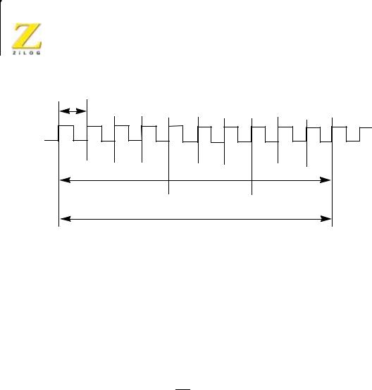
7,0,1*
2YHUYLHZ
7KH = &38 H[HFXWHV LQVWUXFWLRQV E\ VWHSSLQJ WKURXJK D SUHFLVH VHW RI EDVLF RSHUDWLRQV 7KHVH LQFOXGH
•
•
•
Memory Read or Write
I/O Device Read or Write
Interrupt Acknowledge
$OO LQVWUXFWLRQV DUH VHULHV RI EDVLF RSHUDWLRQV (DFK RI WKHVH RSHUDWLRQV FDQ WDNH IURP WKUHH WR VL[ FORFN SHULRGV WR FRPSOHWH RU WKH\ FDQ EH OHQJWKHQHG WR V\QFKURQL]H WKH &38 WR WKH VSHHG RI H[WHUQDO GHYLFHV 7KH FORFN SHULRGV DUH UHIHUUHG WR DV 7 WLPH F\FOHV DQG WKH RSHUDWLRQV DUH UHIHUUHG WR DV 0 PDFKLQH F\FOHV )LJXUH LOOXVWUDWHV KRZ D W\SLFDO LQVWUXFWLRQ LV VHULHV RI VSHFLILF 0 DQG 7 F\FOHV 1RWLFH WKDW WKLV LQVWUXFWLRQ FRQVLVWV RI WKUHH PDFKLQH F\FOHV 0 0 DQG 0 7KH ILUVW PDFKLQH F\FOH RI DQ\ LQVWUXFWLRQ LV D IHWFK F\FOH ZKLFK LV IRXU ILYH RU VL[ 7 F\FOHV ORQJ XQOHVV OHQJWKHQHG E\ WKH :$,7 VLJQDO ZKLFK LV GHVFULEHG LQ WKH QH[W VHFWLRQ 7KH IHWFK F\FOH 0 LV XVHG WR IHWFK WKH RSFRGH RI WKH QH[W LQVWUXFWLRQ WR EH H[HFXWHG 6XEVHTXHQW PDFKLQH F\FOHV PRYH GDWD EHWZHHQ WKH &38 DQG PHPRU\ RU , 2 GHYLFHV DQG WKH\ PD\ KDYH DQ\ZKHUH IURP WKUHH WR ILYH 7 F\FOHV DJDLQ WKH\ PD\ EH OHQJWKHQHG E\ ZDLW VWDWHV WR V\QFKURQL]H WKH H[WHUQDO GHYLFHV WR WKH &38 7KH IROORZLQJ SDUDJUDSKV GHVFULEH WKH WLPLQJ ZKLFK RFFXUV ZLWKLQ DQ\ RI WKH EDVLF PDFKLQH F\FOHV
'XULQJ 7 DQG HYHU\ VXEVHTXHQW 7Z WKH &38 VDPSOHV WKH :$,7 OLQH ZLWK WKH IDOOLQJ HGJH RI &ORFN ,I WKH :$,7 OLQH LV DFWLYH DW WKLV WLPH DQRWKHU :$,7 VWDWH LV HQWHUHG GXULQJ WKH IROORZLQJ F\FOH 8VLQJ WKLV WHFKQLTXH WKH UHDG FDQ EH OHQJWKHQHG WR PDWFK WKH DFFHVV WLPH RI DQ\ W\SH RI PHPRU\ GHYLFH
80 |
2YHUYLHZ |
< %27 7UGT U /CPWCN
7 &\FOH |
|
|
|
|
|
|
|
|
&/. |
|
|
|
|
|
|
|
|
7 |
7 |
7 |
7 |
7 |
7 |
7 |
7 |
7 |
|
0DFKLQH &\FOH |
|
|
|
|
|
|
|
|
0 |
|
|
0 |
|
|
0 |
|
|
2SFRGH )HWFK |
0HPRU\ 5HDG |
|
0HPRU\ :ULWH |
|
|||
|
|
|
,QVWUXFWLRQ &\FOH |
|
|
|
|
|
)LJXUH |
%DVLF &38 7LPLQJ ([DPSOH |
|
|
|
||||
,QVWUXFWLRQ )HWFK
)LJXUH GHSLFWV WKH WLPLQJ GXULQJ DQ 0 RSFRGH IHWFK F\FOH 7KH 3& LV SODFHG RQ WKH DGGUHVV EXV DW WKH EHJLQQLQJ RI WKH 0 F\FOH 2QH KDOI FORFN F\FOH ODWHU WKH 05(4 VLJQDO JRHV DFWLYH $W WKLV WLPH WKH DGGUHVV WR WKH PHPRU\ KDV KDG WLPH WR VWDELOL]H VR WKDW WKH IDOOLQJ HGJH RI 05(4 FDQ EH XVHG GLUHFWO\ DV D FKLS HQDEOH FORFN WR G\QDPLF PHPRULHV 7KH 5' OLQH DOVR JRHV DFWLYH WR LQGLFDWH WKDW WKH PHPRU\ UHDG GDWD VKRXOG EH HQDEOHG RQWR WKH &38 GDWD EXV 7KH &38 VDPSOHV WKH GDWD IURP WKH PHPRU\ RQ WKH GDWD EXV ZLWK WKH ULVLQJ HGJH RI WKH FORFN RI VWDWH 7 DQG WKLV VDPH HGJH LV XVHG E\ WKH &38 WR WXUQ RII WKH 5' DQG 05(4 VLJQDOV 7KXV WKH GDWD KDV DOUHDG\ EHHQ VDPSOHG E\ WKH &38 EHIRUH WKH 5' VLJQDO EHFRPHV LQDFWLYH &ORFN VWDWH 7 DQG 7 RI D IHWFK F\FOH DUH XVHG WR UHIUHVK G\QDPLF PHPRULHV 7KH &38 XVHV WKLV WLPH WR GHFRGH DQG H[HFXWH WKH IHWFKHG LQVWUXFWLRQ VR WKDW QR RWKHU RSHUDWLRQ FRXOG EH SHUIRUPHG DW WKLV WLPH
'XULQJ 7 DQG 7 WKH ORZHU VHYHQ ELWV RI WKH DGGUHVV EXV FRQWDLQ D PHPRU\ UHIUHVK DGGUHVV DQG WKH 5)6+ VLJQDO EHFRPHV DFWLYH WLQGLFDWLQJ WKDW D UHIUHVK UHDG RI DOO G\QDPLF PHPRULHV PXVW EH DFFRPSOLVKHG $Q 5' VLJQDO LV QRW JHQHUDWHG GXULQJ UHIUHVK WLPH WR SUHYHQW GDWD IURP GLIIHUHQW PHPRU\
80 |
2YHUYLHZ |
Loading...