


 Loading...
.
ERTEC 200
Enhanced Real-Time Ethernet Controller
Manual
Copyright © Siemens AG 2007. All rights reserved. |
Page 1 |
Technical data subject to change |
|
ERTEC 200 Manual
Version 1.1.0

Edition (04/2007)
Disclaimer of Liability
We have checked the contents of this manual for agreement with the hardware and software described. Since deviations cannot be precluded entirely, we cannot guarantee full agreement. However, the data in this manual are reviewed regularly. Necessary corrections are included in subsequent editions. Suggestions for improvement are welcomed.
Copyright
© Siemens AG 2006. All rights reserved
The reproduction, transmission or use of this document or its contents is not permitted without express written authority. Offenders will be liable for damages. All rights, including rights created by patent grant or registration of a utility model or design, are reserved.
All product and system names are registered trademarks of their respective owner and must be treated as such.
Technical data subject to change.
Copyright © Siemens AG 2007. All rights reserved. |
Page 2 |
Technical data subject to change |
|
ERTEC 200 Manual
Version 1.1.0

Preface
Target Audience of this Manual
This manual is intended for hardware developers who want to use the ERTEC 200 for new products. Experience working with processors and designing embedded systems and knowledge of Ethernet are required for this. It described all ERTEC function groups in details and provides information that you must take into account when configuring your own PROFINET IO device hardware.
The manual serves as a reference for software developers. The address areas and register contents are described in detail for all function groups.
Structure of this Manual
o Section 1 Overview of the architecture and the individual function groups of the ERTEC 200. o Section 2 ARM946E-S processor systems.
o Section 3 Bus system of the ERTEC 200. o Section 4 I/O of the ERTEC 200.
o Section 5 General hardware functions.
o Section 6 External memory interface (EMIF). o Section 7 Local bus unit (LBU).
o Section 8 DMA controller o Section 9 Ethernet PHYs
o Section 10 Memory partitioning of the ERTEC 200. o Section 11 HW tools for test, trace, and debugging. o Section 12 List of terms and references
Scope of the Manual
This manual applies to the following product:
ERTEC 200 Version 01 and higher
Copyright © Siemens AG 2007. All rights reserved. |
Page 3 |
Technical data subject to change |
|
ERTEC 200 Manual
Version 1.1.0

This manual will be updated as required. You can find the current version of the manual on the Internet at http://www.siemens.com/comdec.
Guide
To help you quickly find the information you need, this manual contains the following aids:
oA complete table of contents as well as a list of all figures and tables in the manual are provided at the beginning of the manual.
o A glossary containing definitions of important terms used in the manual is located following the appendices.
oReferences to other documents are indicated by the document reference number enclosed in slashes (/No./). The complete title of the document can be obtained from the list of references at the end of the manual.
Additional Support
If you have questions regarding use of the described block that are not addressed in the documentation, please contact your Siemens representative.
Please send your written questions, comments, and suggestions regarding the manual to the hotline via the e- mail address indicated above.
In addition, you can receive general information, current product information, FAQs, and downloads pertaining to your application on the Internet at:
http://www.siemens.com/comdec
Technical Contacts for Germany / Worldwide
Siemens AG |
Phone: |
0911/750-2736 |
Automation & |
Phone: |
0911/750-2080 |
Drives |
Fax: |
0911/750-2100 |
E-mail: ComDeC@siemens.com |
||
ComDeC |
|
|
Street address: |
Mailing address: |
|
Würzburgerstr.121 |
P.O. Box 2355 |
|
90766 Fürth |
90713 Fürth |
|
Federal Republic of |
Federal Republic of Germany |
|
Germany |
|
|
Technical Contacts for USA |
|
|
PROFI Interface Center: |
Fax: |
(423)- 2622103 |
One Internet Plaza |
Phone: |
(423)- 2622576 |
PO Box 4991 |
E-mail: profibus.sea@siemens.com |
|
Johnson City, TN 37602-4991 |
|
|
Copyright © Siemens AG 2007. All rights reserved. |
Page 4 |
Technical data subject to change |
|
ERTEC 200 Manual
Version 1.1.0

Contents
1 |
Introduction ............................................................................................................................ |
9 |
||
1.1 |
Applications of the ERTEC 200.............................................................................................................. |
9 |
||
1.2 |
Features of the ERTEC 200 ................................................................................................................... |
9 |
||
1.3 |
Structure of the ERTEC 200................................................................................................................... |
10 |
||
1.4 |
ERTEC 200 Package ............................................................................................................................. |
11 |
||
1.5 |
Signal Function Description.................................................................................................................... |
12 |
||
1.5.1 |
GPIO 0 to 31 and Alternative Functions......................................................................................... |
12 |
||
1.5.2 |
JTAG and Debug ........................................................................................................................... |
13 |
||
1.5.3 |
Trace Port ...................................................................................................................................... |
13 |
||
1.5.4 |
Clock and Reset ............................................................................................................................ |
14 |
||
1.5.5 |
Test Pins........................................................................................................................................ |
14 |
||
1.5.6 |
EMIF (External Memory Interface)................................................................................................. |
14 |
||
1.5.7 |
LBU, MII Interface or ETM Trace Interface .................................................................................... |
16 |
||
1.5.8 |
Ethernet PHY1 and PHY2.............................................................................................................. |
18 |
||
1.5.9 |
Power Supply................................................................................................................................. |
19 |
||
2 |
ARM946E-S Processor .......................................................................................................... |
21 |
||
2.1 |
Structure of ARM946E-S........................................................................................................................ |
21 |
||
2.2 |
Description of ARM946E-S .................................................................................................................... |
22 |
||
2.3 |
Operating Frequency of ARM946E-S..................................................................................................... |
22 |
||
2.4 |
Cache Structure of ARM946E-S............................................................................................................. |
22 |
||
2.5 |
Tightly Coupled Memory (TCM) ............................................................................................................. |
22 |
||
2.6 |
Memory Protection Unit (MPU) .............................................................................................................. |
23 |
||
2.7 |
Bus Interface of ARM946E-S ................................................................................................................. |
23 |
||
2.8 |
ARM946E-S Embedded Trace Macrocell (ETM9).................................................................................. |
23 |
||
2.9 |
ARM Interrupt Controller (ICU)............................................................................................................... |
23 |
||
2.9.1 |
Prioritization of Interrupts ............................................................................................................... |
24 |
||
2.9.2 |
Trigger Modes................................................................................................................................ |
24 |
||
2.9.3 |
Masking the Interrupt Inputs .......................................................................................................... |
24 |
||
2.9.4 |
Software Interrupts for IRQ ............................................................................................................ |
24 |
||
2.9.5 |
Nested Interrupt Structure.............................................................................................................. |
24 |
||
2.9.6 |
EOI End-Of-Interrupt...................................................................................................................... |
24 |
||
2.9.7 |
IRQ Interrupt Sources .................................................................................................................... |
25 |
||
2.9.8 |
FIQ Interrupt Sources .................................................................................................................... |
25 |
||
2.9.9 |
IRQ Interrupts as FIQ Interrupt Sources ........................................................................................ |
26 |
||
2.9.10 |
Interrupt Control Register............................................................................................................... |
26 |
||
2.9.11 |
ICU Register Description ............................................................................................................... |
27 |
||
2.10 ARM946E-S Register ............................................................................................................................. |
31 |
|||
3 |
Bus System of the ERTEC 200.............................................................................................. |
32 |
||
3.1 |
“Multilayer AHB” Communication Bus .................................................................................................... |
32 |
||
3.1.1 |
AHB Arbiter.................................................................................................................................... |
32 |
||
3.1.2 |
AHB Master-Slave Coupling .......................................................................................................... |
32 |
||
3.2 |
APB I/O Bus ........................................................................................................................................... |
32 |
||
4 |
I/O on APB bus ....................................................................................................................... |
33 |
||
4.1 |
BOOT ROM............................................................................................................................................ |
33 |
||
4.1.1 |
Booting from External ROM ........................................................................................................... |
34 |
||
4.1.2 |
Booting via SPI .............................................................................................................................. |
34 |
||
4.1.3 |
Booting via UART .......................................................................................................................... |
34 |
||
4.1.4 |
Booting via LBU ............................................................................................................................. |
34 |
||
4.1.5 |
Memory Swapping ......................................................................................................................... |
34 |
||
4.2 |
General Purpose I/O (GPIO) .................................................................................................................. |
35 |
||
4.2.1 |
Address Assignment of GPIO Registers ........................................................................................ |
36 |
||
4.2.2 |
GPIO Register Description............................................................................................................. |
36 |
||
4.3 |
Timer 0/1/2 ............................................................................................................................................. |
38 |
||
4.3.1 |
Timer 0 and Timer 1....................................................................................................................... |
38 |
||
|
4.3.1.1 |
Timer 0/1 Interrupts............................................................................................................... |
39 |
|
|
4.3.1.2 |
Timer 0/1 Prescaler............................................................................................................... |
39 |
|
|
4.3.1.3 |
Cascading of Timers 0/1 ....................................................................................................... |
39 |
|
4.3.2 |
Timer 2........................................................................................................................................... |
39 |
||
4.3.3 |
Address Assignment of Timer Registers........................................................................................ |
40 |
||
4.3.4 |
Timer Register Description ............................................................................................................ |
40 |
||
4.4 |
F-Timer Function.................................................................................................................................... |
43 |
||
4.4.1 |
Address Assignment of F-Timer Registers .................................................................................... |
44 |
||
Copyright © Siemens AG 2007. All rights reserved. |
Page 5 |
Technical data subject to change |
|
ERTEC 200 Manual
Version 1.1.0

4.4.2 |
F-Timer Register Description ......................................................................................................... |
44 |
|
4.5 |
Watchdog Timers ................................................................................................................................... |
45 |
|
4.5.1 |
Watchdog Timer 0.......................................................................................................................... |
45 |
|
4.5.2 |
Watchdog Timer 1.......................................................................................................................... |
45 |
|
4.5.3 |
Watchdog Interrupt ........................................................................................................................ |
45 |
|
4.5.4 |
WDOUT0_N................................................................................................................................... |
45 |
|
4.5.5 |
WDOUT1_N................................................................................................................................... |
45 |
|
4.5.6 |
Watchdog Registers....................................................................................................................... |
46 |
|
4.5.7 |
Address Assignment of Watchdog Registers................................................................................. |
46 |
|
4.5.8 |
Watchdog Register Description ..................................................................................................... |
46 |
|
4.6 |
UART Interface....................................................................................................................................... |
48 |
|
4.6.1 |
Address Assignment of UART Registers ....................................................................................... |
49 |
|
4.6.2 |
UART Register Description............................................................................................................ |
50 |
|
4.7 |
Synchronous Interface SPI..................................................................................................................... |
54 |
|
4.7.1 |
Address Assignment of SPI Register ............................................................................................. |
55 |
|
4.7.2 |
SPI Register Description................................................................................................................ |
56 |
|
4.8 |
System control register........................................................................................................................... |
58 |
|
4.8.1 |
Address Assignment of System Control Registers ........................................................................ |
58 |
|
4.8.2 |
System Control Register Description ............................................................................................. |
59 |
|
5 |
General Hardware Functions ................................................................................................ |
64 |
|
5.1 |
Clock Generation and Clock Supply....................................................................................................... |
64 |
|
5.1.1 |
Clock Supply in ERTEC 200 .......................................................................................................... |
64 |
|
5.1.2 |
JTAG Clock Supply........................................................................................................................ |
65 |
|
5.1.3 |
Clock Supply for PHYs and Ethernet MACs .................................................................................. |
65 |
|
5.2 |
Reset Logic of the ERTEC 200 .............................................................................................................. |
65 |
|
5.2.1 |
PowerOn reset............................................................................................................................... |
65 |
|
5.2.2 |
Hardware Reset............................................................................................................................. |
66 |
|
5.2.3 |
Watchdog Reset ............................................................................................................................ |
66 |
|
5.2.4 |
Software reset................................................................................................................................ |
66 |
|
5.2.5 |
IRT Switch Reset ........................................................................................................................... |
66 |
|
5.3 |
Address Space and Timeout Monitoring ................................................................................................ |
67 |
|
5.3.1 |
AHB Bus Monitoring....................................................................................................................... |
67 |
|
5.3.2 |
APB Bus Monitoring....................................................................................................................... |
67 |
|
5.3.3 |
EMIF Monitoring ............................................................................................................................ |
67 |
|
5.4 |
Configuration Options on the ERTEC 200.............................................................................................. |
67 |
|
6 |
External Memory Interface (EMIF) ........................................................................................ |
69 |
|
6.1 |
Address Assignment of EMIF Registers................................................................................................. |
70 |
|
6.2 |
EMIF Register Description ..................................................................................................................... |
70 |
|
7 |
Local Bus Unit (LBU). ............................................................................................................ |
74 |
|
7.1 |
Page Range Setting ............................................................................................................................... |
76 |
|
7.2 |
Page Offset Setting ................................................................................................................................ |
76 |
|
7.3 |
LBU Address Mapping ........................................................................................................................... |
77 |
|
7.4 |
Page Control Setting .............................................................................................................................. |
78 |
|
7.5 |
Host Access to the ERTEC200 .............................................................................................................. |
78 |
|
7.5.1 |
LBU Read from ERTEC 200 with separate Read/Write line (LBU_RDY_N active low) ................. |
79 |
|
7.5.2 |
LBU Write to ERTEC 200 with separate Read/Write line (LBU_RDY_N active low)...................... |
80 |
|
7.5.3 |
LBU Read from ERTEC 200 with common Read/Write line (LBU_RDY_N active low) ................. |
81 |
|
7.5.4 |
LBU Write to ERTEC 200 with common Read/Write line (LBU_RDY_N active low)...................... |
82 |
|
7.6 |
Host Interrupt Handling: ......................................................................................................................... |
82 |
|
7.7 |
Address Assignment of LBU Registers .................................................................................................. |
83 |
|
7.8 |
LBU Register Description ....................................................................................................................... |
83 |
|
8 |
DMA-Controller....................................................................................................................... |
85 |
|
8.1 |
DMA Register Address Assignment ....................................................................................................... |
86 |
|
8.2 |
Description of DMA Registers ................................................................................................................ |
86 |
|
9 |
Multiport Ethernet PHY.......................................................................................................... |
88 |
|
10 |
Memory Description............................................................................................................... |
91 |
|
10.1 |
Memory Partitioning of the ERTEC 200 ................................................................................................. |
91 |
|
10.2 |
Detailed Memory Description ................................................................................................................. |
92 |
|
11 |
Test and Debugging............................................................................................................... |
94 |
|
11.1 ETM9 Embedded Trace Macrocell ......................................................................................................... |
94 |
||
11.1.1 |
Trace Modes.................................................................................................................................. |
94 |
|
11.1.2 |
Features of the ETM9 Module ....................................................................................................... |
94 |
|
Copyright © Siemens AG 2007. All rights reserved. |
Page 6 |
Technical data subject to change |
|
ERTEC 200 Manual
Version 1.1.0

11.1.3 ETM9 Registers ............................................................................................................................. |
94 |
|
11.2 |
Trace Interface ....................................................................................................................................... |
95 |
11.3 |
JTAG Interface ....................................................................................................................................... |
95 |
11.4 Debugging via UART.............................................................................................................................. |
95 |
|
12 |
Miscellaneous......................................................................................................................... |
96 |
12.1 |
Acronyms/Glossary: ............................................................................................................................... |
96 |
12.2 |
References:............................................................................................................................................ |
97 |
Copyright © Siemens AG 2007. All rights reserved. |
Page 7 |
Technical data subject to change |
|
ERTEC 200 Manual
Version 1.1.0

List of Figures |
|
Figure 1: ERTEC 200 Block Diagram .................................................................................................................... |
10 |
Figure 2: ERTEC 200 Package Description .......................................................................................................... |
11 |
Figure 3: Structure of ARM946E-S Processor System .......................................................................................... |
21 |
Figure 4: GPIO Cell on GPIO Port [31:0] of the ERTEC 200................................................................................. |
35 |
Figure 5: Block Diagram of F-Counter ................................................................................................................... |
43 |
Figure 6: Watchdog Timing.................................................................................................................................... |
45 |
Figure 7: Block Diagram of UART ......................................................................................................................... |
48 |
Figure 8: Block Diagram of SPI ............................................................................................................................. |
54 |
Figure 9: Clock Generation in ERTEC 200............................................................................................................ |
64 |
Figure 10: Clock Supply of Ethernet Interface ....................................................................................................... |
65 |
Figure 11: Power-Up Phase of the PLL ................................................................................................................. |
66 |
Figure 12: Interconnection of Addresses between Host and ERTEC 200 LBU ..................................................... |
77 |
Figure 13: LBU-Read-Sequence with separate RD/WR line ................................................................................. |
79 |
Figure 14: LBU-Write-Sequence with separate RD/WR line.................................................................................. |
80 |
Figure 15: LBU-Read-Sequence with common RD/WR line.................................................................................. |
81 |
Figure 16: LBU-Write-Sequence with common RD/WR line.................................................................................. |
82 |
List of Tables |
|
Table 1: ERTEC 200 Pin Assignment and Signal Description............................................................................... |
19 |
Table 2: Overview of IRQ Interrupts ...................................................................................................................... |
25 |
Table 3: Overview of FIQ Interrupts....................................................................................................................... |
25 |
Table 4: Overview of Interrupt Control Register..................................................................................................... |
27 |
Table 5: CP15 Registers - Overview ..................................................................................................................... |
31 |
Table 6: Overview of AHB Master-Slave Access................................................................................................... |
32 |
Table 7: Access Type and Data Width of the I/O................................................................................................... |
33 |
Table 8: Selection of Download Source................................................................................................................. |
34 |
Table 9: Overview of GPIO Registers.................................................................................................................... |
36 |
Table 10: Overview of Timer Registers ................................................................................................................. |
40 |
Table 11: Overview of F-Timer Registers .............................................................................................................. |
44 |
Table 12: Overview of WD Registers..................................................................................................................... |
46 |
Table 13: Baud Rates for UART at FUARTCLK=50 MHz ........................................................................................... |
49 |
Table 14: Overview of UART Registers................................................................................................................. |
49 |
Table 15: Overview of SPI Registers..................................................................................................................... |
55 |
Table 16: Overview of System Control Registers .................................................................................................. |
59 |
Table 17: Overview of ERTEC 200 Clocks............................................................................................................ |
64 |
Table 18: Configurations for ERTEC 200 .............................................................................................................. |
68 |
Table 19: Overview of EMIF Registers .................................................................................................................. |
70 |
Table 20: Setting of Various Page Sizes ............................................................................................................... |
76 |
Table 21: Setting of Various Offset Areas ............................................................................................................. |
76 |
Table 22: Address Mapping from the Perspective of an External Host Processor on the LBU Port ...................... |
77 |
Table 23: Summary of Accesses to Address Areas of ERTEC 200....................................................................... |
78 |
Table 24: Host Access to Address Areas of ERTEC 200 ...................................................................................... |
78 |
Table 25: LBU Read access timing with seperate Read/Write line........................................................................ |
79 |
Table 26: LBU Write access timing with seperate Read/Write line........................................................................ |
80 |
Table 27: LBU Read access timing with common Read/Write line........................................................................ |
81 |
Table 28: LBU Write access timing with common Read/Write line ........................................................................ |
82 |
Table 29: Overview of LBU Registers.................................................................................................................... |
83 |
Table 30: DMA Transfer Modes............................................................................................................................. |
85 |
Table 31: I/O Synchronization Signals................................................................................................................... |
85 |
Table 32: Overview of DMA Registers................................................................................................................... |
86 |
Table 33: Partitioning of Memory Areas ................................................................................................................ |
91 |
Table 34: Detailed Description of Memory Segments............................................................................................ |
93 |
Table 35: Pin Assignment of JTAG Interface......................................................................................................... |
95 |
Copyright © Siemens AG 2007. All rights reserved. |
Page 8 |
Technical data subject to change |
|
ERTEC 200 Manual
Version 1.1.0

1 Introduction
The ERTEC 200 is intended for the implementation of PROFINET devices with RT and IRT functionality. With its integrated ARM946 processor and 2-port Ethernet switch with integrated PHYs and the option to connect an external host processor system to a local bus interface, it meets all the requirements for implementing PROFINET devices with integrated switch functionality.
1.1 Applications of the ERTEC 200
Interface connection for high-precision drive control, including for PC-based systemsDistributed I/O with real-time Ethernet interfacing
PROFINET RT and IRT functionality
1.2 Features of the ERTEC 200
The ERTEC 200 is a high-performance Ethernet controller with the following integrated function groups:
•High-performance ARM 946 processor with D-cache, I-cache, D-TCM memory
•Multilayer AHB bus master/slave with AHB arbiter
•IRT switch with 64-Kbyte communication RAM
•2 Ethernet channels with integrated PHYs
•Local Bus Unit (LBU) for connecting an external host processor (with boot capability)
•SDRAM controller
•SRAM controller
•DMA controller, 1-channel
•45 IO, with assignable parameters
•UART (with boot capability)
•SPI (with boot capability)
•3 timers
•F-timer
•Watchdog
•IRQ and FIQ interrupt controller
•PLL with clock generator
•8 Kbytes of BOOT ROM
•304-pin FBGA housing
•Different test functions
•JTAG debug and trace interface
Copyright © Siemens AG 2007. All rights reserved. |
Page 9 |
Technical data subject to change |
|
ERTEC 200 Manual
Version 1.1.0
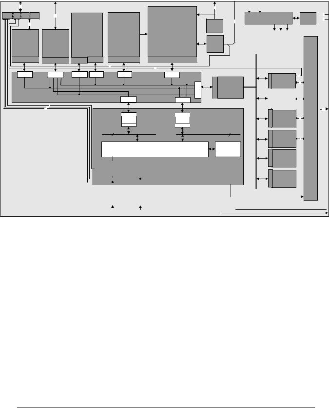
1.3Structure of the ERTEC 200
The figure below shows the function groups with the common communication paths.
LBU / MII + SMI / |
External |
|
|
|
JTAG / Debug |
TRACE_ |
ETM / GPIO |
Memory Interface |
|
|
|
||
|
|
|
CLK |
|||
48 |
|
|
|
|
7 |
|
|
|
|
|
ARM946ES |
|
|
MUX |
74 |
|
|
|
1 |
|
|
|
|
|
|
||
48 |
|
|
ARM- |
with |
BS- |
|
|
|
DMA- |
TAP |
|
||
Local |
|
Interrupt- |
I-Cache (8kByte), |
|
|
|
Memory- |
Controller |
|
|
|||
Bus Unit |
Controller |
D-Cache (4kByte), |
ETM |
|
||
Controller |
|
|
||||
16 Bit |
(EMIF) |
|
|
D-TCM (4kByte) |
Interface |
|
(LBU) |
|
|
|
|
|
|
Master |
Slave |
Master Slave |
Slave |
Master |
|
|
|
|
|
|
14 |
|
|
|
|
|
|
|
|
|
13 |
|
|
|
Input |
MUX/Arb. |
Input |
Decode |
Decode |
Input |
|
|
|
stage |
stage |
stage |
|
|
|
|||
|
|
|
|
|
|
|||
|
|
|
|
|
MUX/Arb. |
AHB/APB |
Master |
|
|
|
|
|
|
Slave |
Bridge |
||
|
|
|
|
|
|
|
|
|
Multi-Layer-AHB |
|
|
Input |
MUX/Arb. |
|
|
|
|
50 MHz/32Bit |
|
|
|
stage |
|
|
|
|
|
|
|
|
|
|
|
||
|
3 |
|
|
|
|
|
|
|
|
16 |
|
|
|
|
|
|
|
|
16 |
|
|
|
|
|
|
|
|
|
|
|
Master |
Slave |
|
|
|
|
|
|
|
AHB- |
AHB- |
|
|
|
|
|
|
|
Wrapper |
Wrapper |
|
|
|
|
|
|
|
Slave |
Master |
|
|
|
|
|
|
|
32 Bit |
MC-Bus (50MHz) |
SC-Bus (50MHz) |
32 Bit |
|
|
|
|
|
|
Switch Control |
K-SRAM |
|
|
|
|
|
|
|
|
64 kByte |
|
|
|
|
|
|
|
|
|
|
|
|
|
|
|
|
|
|
|
|
|
|
|
|
|
|
|
|
|
|
|
Ethernet- |
|
Ethernet- |
|
|
|||
|
|
|
SMI |
|
|
2-Port Switch |
|||||||
|
|
|
|
Port1 |
|
Port2 |
|||||||
|
|
|
|
|
|
|
|||||||
|
|
|
|
|
|
|
|||||||
|
|
|
|
|
|
|
|
|
|
|
|
|
|
|
|
|
|
|
|
|
MII-1 |
|
|
|
|
|
|
|
|
|
|
|
|
|
|
|
|
|
|
|
|
|
|
|
|
MII-0 |
|
|
|
|
|
|
|
|
|
|
|
|
|
|
|
|
|
|
|
|
|
|
|
|
|
|
|
|
|
|
|
|
|
|
|
|
|
|
|
|
|
|
|
|
|
|
|
|
|
|
|
REF_ |
F_CLK |
|
|
|
|
25MHz |
||||||
CLK |
|
|
|
|
|
|
|
|||||
|
|
|
|
|
|
|
|
|
|
|||
|
|
|
|
|
|
|
|
|
|
|
|
|
|
|
|
|
|
|
1 |
|
|
1 |
|
||
|
1 |
|
|
1 |
|
|
|
|
|
|
||
|
|
|
|
|
|
|
|
|
|
|
|
|
|
|
|
|
|
|
|
|
|
|
|
|
|
Clock-Unit PLL
ARM9 clock |
50MHz |
100MHz |
APB
50MHz / 32 Bit
Slave |
|
13 |
GPIO |
32 |
|
|
|
P |
Slave |
1 x UART |
|
|
|
P |
|
|
|
5 |
|
|
|
|
|
|
|
|
|
|
|
|
|
|
Slave |
SPI1 |
o |
|
8 |
|||
Interface |
|||
|
r |
||
|
|
||
Slave |
3 x Timer, |
t |
|
Watchdog, |
|||
2 |
|||
|
F-Timer |
s |
|
|
|
||
Slave |
System |
|
|
Control |
|
||
|
|
Slave |
Boot- |
ROM |
(8 kByte)
PHY |
|
PHY |
|
|
|
|
|
|
|
|
|
||
|
|
|
|
|
7 |
|
|
||||||
|
|
|
|
MC-PLL Signals |
|||||||||
(Port 1) |
|
(Port 2) |
|
|
|
|
|
|
|
|
|||
|
|
|
|
|
|
|
|
|
|||||
|
|
|
|
|
|
|
|
|
|
||||
|
|
|
|
|
|
|
|
|
|
|
|
|
|
|
|
|
|
|
|
|
|
|
|
|
|
|
|
|
|
|
|
|
|
|
|
21 |
|
|
|
|
|
|
|
|
|
|
|
|
|
|
|
|
|
|
|
|
|
|
|
|
|
|
|
|
|
|
|
|
|
|
|
|
|
|
|
20 |
|
|
|
|
|
|
|
|
|
|
|
|
|
|
|
|
|
|
|
|
|
 1 Reset
 4 Test
GPIO,
UART,  32 SPI,
Timer,
Watchdog,
 PHY2
PHY2
PHY1
ERTEC200
Figure 1: ERTEC 200 Block Diagram
Copyright © Siemens AG 2007. All rights reserved. |
Page 10 |
Technical data subject to change |
|
ERTEC 200 Manual
Version 1.1.0

1.4ERTEC 200 Package
The ERTEC 200 is supplied in an FBGA package with 304 pins. The distance between the pins is 0.8 mm. The package dimensions are 19 mm x 19 mm.
Figure 2: ERTEC 200 Package Description
Soldering instructions for the ERTEC 200 can be found in the following documents: /10/ Soldering instructions for lead-based block.
/11/ Soldering instructions for lead-free block. /12/ Code description for soldering.
When working with modules, always take precautionary measures against electrostatic charge (ESD – Electrostatic Sensitive Devices).
Copyright © Siemens AG 2007. All rights reserved. |
Page 11 |
Technical data subject to change |
|
ERTEC 200 Manual
Version 1.1.0

1.5Signal Function Description
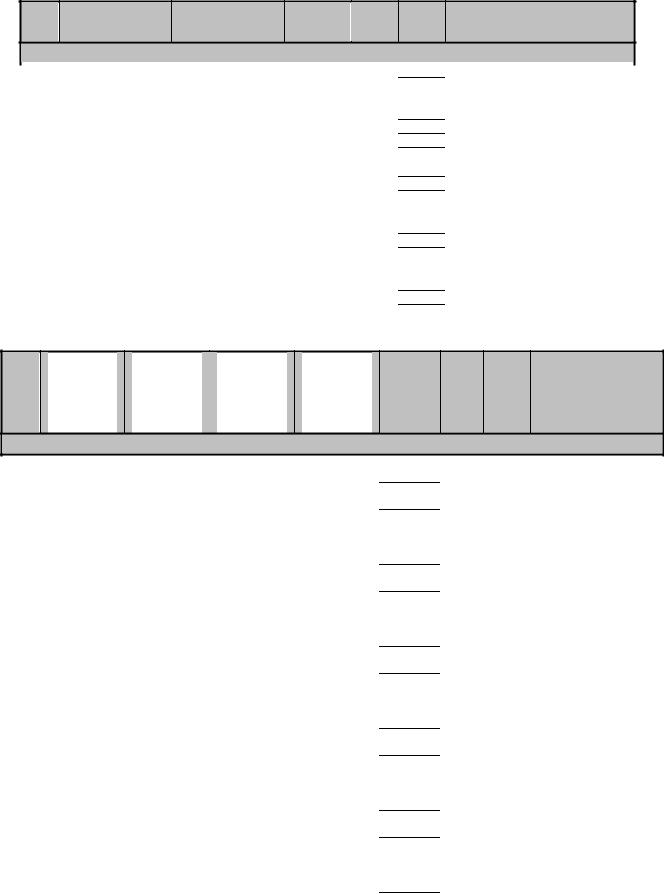
ERTEC 200 Pin Description
The ERTEC 200 Ethernet communication block is available in a 304-pin FBGA package. The signal names of the ERTEC 200 are described in this section.
1.5.1GPIO 0 to 31 and Alternative Functions
Various signals are multiplexed on the same pin. These multiplexed signals can contain up to four different functions. The alternative functions are assigned in GPIO registers GPIO_PORT_MODE_L and GPIO_PORT_MODE_H (see Section 4.2.2). The table describes all signals with their different functions and associated pin numbers.
No. |
|
Signal |
|
Alternative |
Alternative |
|
Alternative |
I/O |
Pull- |
PIN |
Comment |
|
|
Name |
|
Function 1 |
Function 2 |
|
Function 3 |
(Reset) |
|
No. |
|
|
|
|
|
|
|
|
|
|
|
|
|
|
|
|
|
|
General Purpose I/O / I/O |
|
|
|
|||
|
|
|
|
|
|
|
|
|
|
|
|
1 |
|
GPIO0 |
|
P1-DUBLEX- |
|
|
|
B/O/(I) |
up |
D19 |
GPIO (interrupt- |
|
|
|
LED_N |
|
|
|
|
|
|
capable) or PHY-LED |
|
|
|
|
|
|
|
|
|
|
|
|
(O) |
2 |
|
GPIO1 |
|
P2-DUBLEX- |
|
|
|
B/O/(I) |
up |
B20 |
GPIO (interrupt- |
|
|
|
LED_N |
|
|
|
|
|
|
capable) or PHY-LED |
|
|
|
|
|
|
|
|
|
|
|
|
(O) |
3 |
|
GPIO2 |
|
P1-SPEED_N- |
P1-SPEED- |
|
|
B/O/O/(I) |
up |
D17 |
GPIO or PHY-LED (O) |
|
|
|
100LED |
10LED_N |
|
|
|
|
|
|
|
|
|
|
|
(TX/FX) |
|
|
|
|
|
|
|
|
|
GPIO3 |
|
P2-SPEED- |
P2-SPEED- |
|
|
B/O/O/(I) |
up |
B19 |
GPIO or PHY-LED (O) |
4 |
|
|
|
100LED_N |
10LED_N |
|
|
|
|
|
|
|
|
|
|
(TX/FX) |
|
|
|
|
|
|
|
5 |
|
GPIO4 |
|
P1-LINK- |
|
|
|
B/O/(I) |
up |
A19 |
GPIO or PHY-LED (O) |
|
|
|
LED_N |
|
|
|
|
|
|
|
|
|
|
|
|
|
|
|
|
|
|
|
|
6 |
|
GPIO5 |
|
P2-LINK- |
|
|
|
B/O/(I) |
up |
D16 |
GPIO or PHY-LED (O) |
|
|
|
LED_N |
|
|
|
|
|
|
|
|
|
|
|
|
|
|
|
|
|
|
|
|
7 |
|
GPIO6 |
|
P1-RX-LED_N |
P1-TX-LED_N |
|
P1-ACTIVE- |
B/O/O/O/(I) |
up |
B18 |
GPIO or PHY-LED (O) |
|
|
|
|
|
|
LED_N |
|
|
|
|
|
|
|
|
|
|
|
|
|
|
|
|
|
8 |
|
GPIO7 |
|
P2-RX-LED_N |
P2-TX-LED_N |
|
P2-ACTIVE- |
B/O/O/O/(I) |
up |
D15 |
GPIO or PHY-LED (O) |
|
|
|
|
|
|
LED_N |
|
|
|
|
|
|
|
|
|
|
|
|
|
|
|
|
|
9 |
|
GPIO8 |
|
UART-TXD |
|
|
|
B/O/(I) |
up |
B17 |
GPIO or UART (O) |
|
|
|
|
|
|
|
|
|
|
|
|
|
|
|
|
|
|
|
|
|
|
|
|
10 |
|
GPIO9 |
|
UART-RXD |
|
|
|
B/I (I) |
up |
A17 |
GPIO or UART (I) |
|
|
|
|
|
|
|
|
|
|
|
|
11 |
|
GPIO10 |
|
UART-DCD_N |
|
|
|
B/I (I) |
up |
B16 |
GPIO or UART (I) |
|
|
|
|
|
|
|
|
|
|
|
|
12 |
|
GPIO11 |
|
UART-DSR_N |
|
|
|
B/I (I) |
up |
E16 |
GPIO or UART (I) |
|
|
|
|
|
|
|
|
|
|
|
|
13 |
|
GPIO12 |
|
UART-CTS_N |
|
|
|
B/I (I) |
up |
A16 |
GPIO or UART (I) |
|
|
|
|
|
|
|
|
|
|
|
|
14 |
|
GPIO13 |
|
Reserved |
|
|
|
B/O/(I) |
up |
B15 |
GPIO |
|
|
|
|
|
|
|
|
|
|
|
|
15 |
|
GPIO14 |
|
DBGACK |
|
|
|
B/O/(I) |
up |
E15 |
GPIO or DEBUG (O) |
|
|
|
|
|
|
|
|
|
|
|
|
16 |
|
GPIO15 |
|
WD_WDOUT0_ |
|
|
|
B/O/(I) |
up |
E14 |
GPIO or Watchdog (O) |
|
|
|
|
N |
|
|
|
|
|
|
|
17 |
|
GPIO16 |
|
SPI1_SSPCTL |
|
|
|
B/O/(I) |
up |
A13 |
GPIO or SPI1 (O) |
|
|
|
|
OE |
|
|
|
|
|
|
|
18 |
|
GPIO17 |
|
SPI1_SSPOE |
|
|
|
B/O/(I) |
up |
F14 |
GPIO or SPI1 (O) |
|
|
|
|
|
|
|
|
|
|
|
|
19 |
|
GPIO18 |
|
SPI1_SSPRXD |
|
|
|
B/I (I) |
up |
B12 |
GPIO or SPI1 (I) |
|
|
|
|
|
|
|
|
|
|
|
|
20 |
|
GPIO19 |
|
SPI1_SSPTXD |
|
|
|
B/O/(I) |
up |
D13 |
GPIO or SPI1 (O) |
|
|
|
|
|
|
|
|
|
|
|
|
21 |
|
GPIO20 |
|
SPI1_SCLKOU |
|
|
|
B/O/(I) |
up |
D11 |
GPIO or SPI1 (O) |
|
|
|
|
T |
|
|
|
|
|
|
|
22 |
|
GPIO21 |
|
SPI1_SFRMOU |
|
|
|
B/O/(I) |
up |
A11 |
GPIO or SPI1 (O) |
|
|
|
|
T |
|
|
|
|
|
|
|
Copyright © Siemens AG 2007. All rights reserved. |
12 |
ERTEC 200 Manual |
Technical data subject to change |
|
Version 1.1.0 |
No. |
Signal |
Alternative |
Alternative |
Alternative |
I/O |
Pull- |
PIN |
Comment |
|
Name |
Function 1 |
Function 2 |
Function 3 |
(Reset) |
|
No. |
|
|
|
|
|
|
|
|
|
|
|
|
|
General Purpose I/O / I/O |
|
|
|
||
|
|
|
|
|
|
|
|
|
23 |
GPIO22 |
SPI1_SFRMIN |
DBGACK |
|
B/I/O/(I) |
up |
F10 |
GPIO or SPI1 (I) or |
|
|
|
|
|
|
|
|
Debug (O) |
|
|
|
|
|
|
|
|
This GPIO is used as |
|
|
|
|
|
|
|
|
chip select when |
|
|
|
|
|
|
|
|
booting from Nand |
|
|
|
|
|
|
|
|
Flash or SPI ROM. |
24 |
GPIO23 |
SPI1_SCLKIN |
Reserved |
|
B/I/O/(I) |
up |
D10 |
GPIO or SPI1 (I) |
|
|
|
|
|
|
|
|
This GPIO is used as |
|
|
|
|
|
|
|
|
chip select when |
|
|
|
|
|
|
|
|
booting from SPI Flash |
|
|
|
|
|
|
|
|
or SPI EEPROM. |
25 |
GPIO24 |
PLL_EXT_IN_N |
|
|
B/I (I) |
up |
B11 |
GPIO or MC_PLL (I) |
26 |
GPIO25 |
TGEN_OUT1_N |
|
|
B/O/(I) |
up |
B9 |
GPIO or MC_PLL (O) |
|
|
*1 |
|
|
|
|
|
|
27 |
GPIO26 |
TGEN_OUT2_N |
|
|
B/O/(I) |
up |
A7 |
GPIO or MC_PLL (O) |
28 |
GPIO27 |
TGEN_OUT3_N |
|
|
B/O/(I) |
up |
B10 |
GPIO or MC_PLL (O) |
29 |
GPIO28 |
TGEN_OUT4_N |
|
|
B/O/(I) |
up |
F9 |
GPIO or MC_PLL (O) |
30 |
GPIO29 |
TGEN_OUT5_N |
|
|
B/O/(I) |
up |
E9 |
GPIO or MC_PLL (O) |
31 |
GPIO30 |
TGEN_OUT6_N |
|
|
B/O/(I) |
up |
B8 |
GPIO (interrupt- |
|
|
|
|
|
|
|
|
capable) or MC_PLL |
|
|
|
|
|
|
|
|
(O) |
32 |
GPIO31 |
DBGREQ |
|
|
B/I (I) |
up |
E8 |
GPIO (interrupt- |
|
|
|
|
|
|
|
|
capable) or DEBUG (I) |
*1 For an IRT application pin GPIO25 is default parameterized as alternate function1 (TGEN_OUT1_N). A synchronous clock is issued at this pin. During the certification process of a PROFINET IO DEVICE with IRT functionality this pin has to be accessible from outside (mandatory).
Different GPIO’s are used on the Evaluation Board EB200. See Dokument /14/ Table 6.
1.5.2JTAG and Debug
No. |
Signal |
I/O |
Pull- |
PIN |
Comment |
|
Name |
(Reset) |
|
No. |
|
|
|
|
|
|
|
|
|
Debug / JTAG (BOUNDARY SCAN) |
|||
|
|
|
|
|
|
33 |
TRST_N |
I (I) |
|
U10 |
JTAG Reset |
34 |
TCK |
I (I) |
up |
W7 |
JTAG Clock |
35 |
TDI |
I (I) |
up |
U9 |
JTAG Data In |
36 |
TMS |
I (I) |
up |
V7 |
JTAG Test Mode Select |
37 |
TDO |
O (O) |
|
V9 |
JTAG Data Out |
38 |
SRST_N |
B (O) |
up |
V8 |
Hardware Reset |
39 |
TAP_SEL |
I (I) |
up |
W8 |
Select TAP Controller: |
|
|
|
|
|
0: Boundary Scan TAP Controller |
|
|
|
|
|
selected |
|
|
|
|
|
1: ARM-TAP Controller selected |
|
|
|
|
|
or Scan Clock (Scan mode) |
1.5.3Trace Port
No. |
Signal |
I/O |
|
Pull- |
PIN |
Comment |
|
Name |
(Reset) |
|
|
No. |
|
|
|
|
|
|
|
|
|
|
|
Trace Port/Other |
|
||
|
|
|
|
|
|
|
40 |
TRACECLK |
B (O) |
|
|
AB4 |
ETM Trace Clock |
41 |
Reserved |
I (I) |
|
up |
U19 |
Connect pin to GND |
Copyright © Siemens AG 2007. All rights reserved. |
13 |
ERTEC 200 Manual |
Technical data subject to change |
|
Version 1.1.0 |

1.5.4Clock and Reset
|
No. |
|
|
Signal Name |
|
|
I/O |
|
|
Pull- |
|
|
PIN |
|
|
Comment |
|
|
|
|
|
|
|
|
(Reset) |
|
|
|
|
|
No. |
|
|
|
|
|
|
|
|
|
|
|
|
|
|
|
|
|
|
|
|
|
|
|
|
|
|
|
|
|
CLOCK / RESET GENERATION |
|
|||||||||
|
|
|
|
|
|
|
|
|
|
|
|
|
|
|
|
|
|
42 |
|
CLKP_A |
|
I (I) |
|
|
|
|
B14 |
|
Quartz connection |
||||||
43 |
|
|
CLKP_B |
|
O |
|
|
|
|
D14 |
|
Quartz connection |
|||||
44 |
|
F_CLK |
|
I (I) |
|
|
|
|
B13 |
|
F_CLK for F-counter |
||||||
45 |
|
|
REF_CLK |
|
Dependent |
|
|
|
|
A15 |
|
Tristate or |
|||||
|
|
|
|
|
|
|
on PIN |
|
|
|
|
|
|
|
reference clock output, 25 MHz |
||
|
|
|
|
|
|
|
CONFIG[1] |
|
|
|
|
|
|
|
|
|
|
46 |
|
|
RESET_N |
|
I (I) |
|
up |
|
B7 |
|
PowerOn reset |
||||||
1.5.5Test Pins
No. |
Signal Name |
I/O |
Pull- |
PIN |
Comment |
|
|
|
|
(Reset) |
|
No. |
|
|
|
|
|
|
|
|
|
|
|
|
TEST |
|
|
|
|
|
|
|
|
|
47 |
TEST_N |
(3) |
I (I) |
up |
T5 |
Test mode |
48 |
TMC1 |
(3) |
I (I) |
|
G5 |
Test configuration |
49 |
TMC2 |
(3) |
I (I) |
|
H6 |
Test configuration |
50 |
TACT_N |
(3) |
I (I) |
dn |
J5 |
TESTACT-TAP reset |
1.5.6EMIF (External Memory Interface)
No. |
Signal Name |
Alternative |
I/O |
Pull- |
PIN |
Comment |
|
|
Reset Function |
(Reset) |
|
No. |
|
EMIF (External Memory Interface)
51 |
DTR_N |
BOOT0 |
B (I) |
up |
E7 |
Direction signal for external driver |
|
|
|
|
|
|
or scan clock (Scan mode) |
|
|
|
|
|
|
ERTEC 200 boot mode (external |
|
|
|
|
|
|
PD may be necessary) |
|
|
|
|
|
D8 |
|
52 |
OE_DRIVER_N |
|
O (O) |
|
Enable signal for external driver |
|
|
|
|
|
|
B4 |
or scan clock (Scan mode) |
53 |
A0 |
|
O (O) |
|
Address bit 0 |
|
|
|
|
|
|
SDRAM: Bank address 0 |
|
|
|
|
|
|
A3 |
|
54 |
A1 |
|
O (O) |
|
Address bit 1 |
|
|
|
|
|
|
SDRAM: Bank address 1 |
|
|
|
|
|
|
B3 |
|
55 |
A2 |
|
O (O) |
|
Address bit 2 |
|
|
|
|
|
|
SDRAM: Address 0 |
|
|
|
|
|
|
B2 |
|
56 |
A3 |
|
O (O) |
|
Address bit 3 |
|
|
|
|
|
|
SDRAM: Address 1 |
|
|
|
|
|
|
D4 |
|
57 |
A4 |
|
O (O) |
|
Address bit 4 |
|
|
|
|
|
|
SDRAM: Address 2 |
|
|
|
|
|
|
C2 |
|
58 |
A5 |
|
O (O) |
|
Address bit 5 |
|
|
|
|
|
|
SDRAM: Address 3 |
|
|
|
|
|
|
C1 |
|
59 |
A6 |
|
O (O) |
|
Address bit 6 |
|
|
|
|
|
|
SDRAM: Address 4 |
|
|
|
|
|
|
D2 |
|
60 |
A7 |
|
O (O) |
|
Address bit 7 |
|
|
|
|
|
|
SDRAM: Address 5 |
|
|
|
|
|
|
D1 |
|
61 |
A8 |
|
O (O) |
|
Address bit 8 |
|
|
|
|
|
|
SDRAM: Address 6 |
|
|
|
|
|
|
E2 |
|
62 |
A9 |
|
O (O) |
|
Address bit 9 |
|
|
|
|
|
|
SDRAM: Address 7 |
|
|
|
|
|
|
E1 |
|
63 |
A10 |
|
O (O) |
|
Address bit 10 |
|
|
|
|
|
|
SDRAM: Address 8 |
|
|
|
|
|
|
F2 |
|
64 |
A11 |
|
O (O) |
|
Address bit 11 |
|
|
|
|
|
|
SDRAM: Address 9 |
|
|
|
|
|
|
F1 |
|
65 |
A12 |
|
O (O) |
|
Address bit 12 |
|
|
|
|
|
|
SDRAM: Address 10 |
|
|
|
|
|
|
|
Copyright © Siemens AG 2007. All rights reserved. |
14 |
ERTEC 200 Manual |
Technical data subject to change |
|
Version 1.1.0 |

No. |
Signal Name |
Alternative |
I/O |
Pull- |
PIN |
Comment |
|
|
Reset Function |
(Reset) |
|
No. |
|
EMIF (External Memory Interface)
|
66 |
A13 |
|
O (O) |
|
|
G2 |
Address bit 13 |
|
|
|
|
|
|
|
|
|
SDRAM: Address 11 |
|
|
|
|
|
|
|
|
|
|
G1 |
|
||
|
67 |
A14 |
|
O (O) |
|
|
Address bit 14 |
|
|
|
|
|
|
|
|
|
|
SDRAM: Address 12 |
|
|
|
|
|
|
|
|
|
|
H2 |
|
||
|
68 |
A15 |
BOOT1 |
B (I) |
|
dn |
Address bit 15 |
|
|
|
|
|
|
|
|
|
|
|
ERTEC 200 boot mode (ext. PU |
|
|
|
|
|
|
|
|
|
J2 |
may be necessary) |
|
|
|
69 |
A16 |
BOOT2 |
B (I) |
|
dn |
Address bit 16 / |
|
|
|
|
|
|
|
|
|
|
|
ERTEC 200 boot mode (ext. PU |
|
|
|
|
|
|
|
|
|
K2 |
may be necessary) |
|
|
|
70 |
A17 |
BOOT3 |
B (I) |
|
up |
Address bit 17 / |
|
|
|
|
|
|
|
|
|
|
|
ERTEC 200 boot mode (ext. PD |
|
|
|
|
|
|
|
|
|
K1 |
may be necessary) |
|
|
|
71 |
A18 |
CONFIG1 |
B (I) |
|
up |
Address bit 18 / ERTEC 200 |
|
|
|
|
|
|
|
|
|
|
|
system configuration (external PD |
|
|
|
|
|
|
|
|
|
E4 |
may be necessary) |
|
|
|
72 |
A19 |
CONFIG2 |
B (I) |
|
up |
Address bit 19 / ERTEC 200 |
|
|
|
|
|
|
|
|
|
|
|
system configuration (external PD |
|
|
|
|
|
|
|
|
|
F4 |
may be necessary) |
|
|
|
73 |
A20 |
CONFIG3 |
B (I) |
|
dn |
Address bit 20 / ERTEC 200 |
|
|
|
|
|
|
|
|
|
|
|
system configuration (external PU |
|
|
|
|
|
|
|
|
|
G4 |
may be necessary) |
|
|
|
74 |
A21 |
CONFIG4 |
B (I) |
|
up |
Address bit 21 / ERTEC 200 |
|
|
|
|
|
|
|
|
|
|
|
system configuration (external PD |
|
|
|
|
|
|
|
|
|
H5 |
may be necessary) |
|
|
|
75 |
A22 |
CONFIG5 |
B (I) |
|
dn |
Address bit 22 / ERTEC 200 |
|
|
|
|
|
|
|
|
|
|
|
system configuration (external PU |
|
|
|
|
|
|
|
|
|
H4 |
may be necessary) |
|
|
|
76 |
A23 |
CONFIG6 |
B (I) |
|
up |
Address bit 23 / ERTEC 200 |
|
|
|
|
|
|
|
|
|
|
|
system configuration (external PD |
|
|
|
|
|
|
|
|
|
M2 |
may be necessary) |
|
|
|
77 |
D0 |
|
B (I) |
|
up |
Data bit 0 |
|
|
|
|
78 |
D1 |
|
B (I) |
|
up |
N2 |
Data bit 1 |
|
|
|
79 |
D2 |
|
B (I) |
|
up |
P1 |
Data bit 2 |
|
|
|
80 |
D3 |
|
B (I) |
|
up |
P2 |
Data bit 3 |
|
|
|
81 |
D4 |
|
B (I) |
|
up |
R1 |
Data bit 4 |
|
|
|
82 |
D5 |
|
B (I) |
|
up |
T2 |
Data bit 5 |
|
|
|
83 |
D6 |
|
B (I) |
|
up |
U1 |
Data bit 6 |
|
|
|
84 |
D7 |
|
B (I) |
|
up |
U2 |
Data bit 7 |
|
|
|
85 |
D8 |
|
B (I) |
|
up |
V2 |
Data bit 8 |
|
|
|
86 |
D9 |
|
B (I) |
|
up |
W1 |
Data bit 9 |
|
|
|
87 |
D10 |
|
B (I) |
|
up |
W2 |
Data bit 10 |
|
|
|
88 |
D11 |
|
B (I) |
|
up |
Y2 |
Data bit 11 |
|
|
|
89 |
D12 |
|
B (I) |
|
up |
AA1 |
Data bit 12 |
|
|
|
90 |
D13 |
|
B (I) |
|
up |
AA2 |
Data bit 13 |
|
|
|
91 |
D14 |
|
B (I) |
|
up |
AB2 |
Data bit 14 |
|
|
|
92 |
D15 |
|
B (I) |
|
up |
AA3 |
Data bit 15 |
|
|
|
93 |
D16 |
|
B (I) |
|
up |
K4 |
Data bit 16 |
|
|
|
94 |
D17 |
|
B (I) |
|
up |
K5 |
Data bit 17 |
|
|
|
95 |
D18 |
|
B (I) |
|
up |
J6 |
Data bit 18 |
|
|
|
96 |
D19 |
|
B (I) |
|
up |
K6 |
Data bit 19 |
|
|
|
97 |
D20 |
|
B (I) |
|
up |
N5 |
Data bit 20 |
|
|
|
98 |
D21 |
|
B (I) |
|
up |
N6 |
Data bit 21 |
|
|
|
99 |
D22 |
|
B (I) |
|
up |
P6 |
Data bit 22 |
|
|
|
100 |
D23 |
|
B (I) |
|
up |
R5 |
Data bit 23 |
|
|
|
101 |
D24 |
|
B (I) |
|
up |
R6 |
Data bit 24 |
|
|
|
102 |
D25 |
|
B (I) |
|
up |
P4 |
Data bit 25 |
|
|
|
103 |
D26 |
|
B (I) |
|
up |
R4 |
Data bit 26 |
|
|
|
104 |
D27 |
|
B (I) |
|
up |
T4 |
Data bit 27 |
|
|
|
105 |
D28 |
|
B (I) |
|
up |
U4 |
Data bit 28 |
|
|
|
106 |
D29 |
|
B (I) |
|
up |
W4 |
Data bit 29 |
|
|
|
107 |
D30 |
|
B (I) |
|
up |
W5 |
Data bit 30 |
|
|
|
108 |
D31 |
|
B (I) |
|
up |
W6 |
Data bit 31 |
|
|
|
|
|
|
|
|
|
||||
|
Copyright © Siemens AG 2007. All rights reserved. |
|
15 |
|
|
ERTEC 200 Manual |
||||
|
Technical data subject to change |
|
|
|
|
Version 1.1.0 |
||||
No. |
Signal Name |
Alternative |
I/O |
Pull- |
PIN |
Comment |
|
|
Reset Function |
(Reset) |
|
No. |
|
EMIF (External Memory Interface)
109 |
WR_N |
|
O (O) |
|
A4 |
Write strobe |
110 |
RD_N |
|
O (O) |
|
B5 |
Read strobe |
111 |
CS_PER0_N |
|
O (O) |
|
D5 |
Chip Select Bank 1 (ROM); |
|
|
|
|
|
boot area |
|
|
|
|
|
|
A5 |
|
112 |
CS_PER1_N |
|
O (O) |
|
Chip select bank 2 |
|
113 |
CS_PER2_N |
|
O (O) |
|
A6 |
Chip select bank 3 |
114 |
CS_PER3_N |
|
O (O) |
|
B6 |
Chip select bank 4 |
115 |
BE0_DQM0_N |
|
O (O) |
|
N4 |
Byte enable 0 for D(7:0) |
116 |
BE1_DQM1_N |
|
O (O) |
|
V1 |
Byte enable 1 for D(15:8) |
117 |
BE2_DQM2_N |
|
O (O) |
|
J4 |
Byte enable 2 for D(23:16) |
118 |
BE3_DQM3_N |
|
O (O) |
|
P5 |
Byte enable 3 for D(31:24) |
119 |
RDY_PER_N |
|
I (I) |
up |
D7 |
Ready signal |
120 |
CLK_SDRAM |
|
B (O) |
|
M1 |
Clock for SDRAM |
121 |
CS_SDRAM_N |
|
O (O) |
|
L1 |
Chip-Select for SDRAM |
122 |
RAS_SDRAM_N |
|
O (O) |
|
M5 |
RAS for SDRAM |
123 |
CAS_SDRAM_N |
|
O (O) |
|
L2 |
CAS for SDRAM |
124 |
WE_SDRAM_N |
|
O (O) |
|
M4 |
Write Enable for SDRAM |
1.5.7LBU, MII Interface or ETM Trace Interface
No. |
Function 1 |
Function 2 |
Function 3 |
Function 4 |
IO |
Pull |
PIN |
Comment |
|
LBU |
PHY Debug |
ETM Trace |
|
(Reset |
- |
No. |
|
|
|
and |
and |
|
See |
|
|
|
|
|
GPIO[44:32] |
GPIO[44:32] |
Reserved |
Config |
|
|
|
|
Config |
Config |
Config |
|
[6,5,2]) |
|
|
|
|
(6,5,2)=xx0b |
(6,5,2)=011b |
(6,5,2)=101b |
[6,5,2]=111b |
|
|
|
|
LBU / MII Interface/ ETM Trace Interface
125 |
LBU_A0 |
RXD_P10 |
ETMEXTOUT |
|
|
|
|
|
|
126 |
LBU_A1 |
RXD_P11 |
ETMEXTIN1 |
|
|
|
|
|
|
127 |
LBU_A2 |
RXD_P12 |
TRACEPKT7 |
|
|
|
|
|
|
128 |
LBU_A3 |
RXD_P13 |
TRACEPKT6 |
|
|
|
|
|
|
129 |
LBU_A4 |
CRS_P1 |
TRACEPKT5 |
|
|
|
|
|
|
130 |
LBU_A5 |
RX_ER_P1 |
TRACEPKT4 |
|
|
|
|
|
|
131 |
LBU_A6 |
RX_DV_P1 |
TRACEPKT3 |
|
|
|
|
|
|
132 |
LBU_A7 |
COL_P1 |
TRACEPKT2 |
|
|
|
|
|
|
133 |
LBU_A8 |
RXD_P20 |
TRACEPKT1 |
|
|
|
|
|
|
134 |
LBU_A9 |
RXD_P21 |
TRACEPKT0 |
|
|
|
|
|
|
135 |
LBU_A10 |
RXD_P22 |
TRACESYNC |
|
|
|
|
|
|
136 |
LBU_A11 |
RXD_P23 |
PIPESTA2 |
|
|
|
|
|
|
137 |
LBU_A12 |
CRS_P2 |
PIPESTA1 |
|
|
|
|
|
|
138 |
LBU_A13 |
RX_ER_P2 |
PIPESTA0 |
|
|
|
|
|
|
139 |
LBU_A14 |
RX_DV_P2 |
|
|
|
|
|
|
|
140 |
LBU_A15 |
COL_P2 |
|
|
|
|
|
|
|
I/O/O/I |
up |
AB3 |
LBU or MII or ETM |
(ETM : I) |
|
|
|
I/O/I/I |
up |
AA4 |
LBU or MII or ETM |
(ETM : I) |
|
|
|
I/O/O/I |
up |
AA5 |
LBU or MII or ETM |
(ETM : I) |
|
|
|
I/O/O/I |
up |
AB5 |
LBU or MII or ETM |
(ETM : I) |
|
|
|
I/O/O/I |
up |
AA6 |
LBU or MII or ETM |
(ETM : I) |
|
|
|
I/O/O/I |
up |
AB6 |
LBU or MII or ETM |
(ETM : I) |
|
|
|
I/O/O/I |
up |
AA7 |
LBU or MII or ETM |
(ETM : I) |
|
|
|
I/O/O/I |
up |
AB7 |
LBU or MII or ETM |
(ETM : I) |
|
|
|
I/O/O/I |
up |
AA8 |
LBU or MII or ETM |
(ETM : I) |
|
|
|
I/O/O/I |
up |
AB8 |
LBU or MII or ETM |
(ETM : I) |
|
|
|
I/O/O/I |
up |
AA9 |
LBU or MII or ETM |
(ETM : I) |
|
|
|
I/O/O/I |
up |
AA10 |
LBU or MII or ETM |
(ETM : I) |
|
|
|
I/O/O/I |
up |
AB10 |
LBU or MII or ETM |
(ETM : I) |
|
|
|
I/O/O/I |
up |
AA11 |
LBU or MII or ETM |
(ETM : I) |
|
|
|
I/O/I/I |
up |
AB11 |
LBU or MII |
I/O/I/I |
|
|
|
up |
W11 |
LBU or MII |
|
|
|
|
|
Copyright © Siemens AG 2007. All rights reserved. |
16 |
ERTEC 200 Manual |
Technical data subject to change |
|
Version 1.1.0 |

No. |
Function 1 |
Function 2 |
Function 3 |
Function 4 |
IO |
Pull |
PIN |
Comment |
|
LBU |
PHY Debug |
ETM Trace |
|
(Reset |
- |
No. |
|
|
|
and |
and |
|
See |
|
|
|
|
|
GPIO[44:32] |
GPIO[44:32] |
Reserved |
Config |
|
|
|
|
Config |
Config |
Config |
|
[6,5,2]) |
|
|
|
|
(6,5,2)=xx0b |
(6,5,2)=011b |
(6,5,2)=101b |
[6,5,2]=111b |
|
|
|
|
LBU / MII-Interface
141 |
LBU_A16 |
GPIO32 |
GPIO32 |
|
|
|
|
142 |
LBU_A17 |
GPIO33 |
GPIO33 |
|
|
|
|
143 |
LBU_A18 |
GPIO34 |
GPIO34 |
|
|
|
|
144 |
LBU_A19 |
GPIO35 |
GPIO35 |
|
|
|
|
145 |
LBU_A20 |
GPIO36 |
GPIO36 |
|
|
|
|
146 |
LBU_SEG_0 |
GPIO37 |
GPIO37 |
|
|
|
|
147 |
LBU_SEG_1 |
GPIO38 |
GPIO38 |
|
|
|
|
148 |
LBU_WR_N |
TX_CLK_P1 |
|
149 LBU_RD_N TX_CLK_P2
150 |
LBU_CS_R_ |
GPIO39 |
GPIO39 |
|
N |
|
|
|
|
|
|
151 |
LBU_CS_M_ |
GPIO40 |
GPIO40 |
|
N |
|
|
152LBU_BE0_N RX_CLK_P1
153LBU_BE1_N RX_CLK_P2
154 |
LBU_D0 |
TXD_P10 |
|
|
|
155 |
LBU_D1 |
TXD_P11 |
|
|
|
156 |
LBU_D2 |
TXD_P12 |
|
|
|
157 |
LBU_D3 |
TXD_P13 |
|
|
|
158 |
LBU_D4 |
TX_EN_P1 |
|
|
|
159 |
LBU_D5 |
TX_ERR_P1 |
|
|
|
160 |
LBU_D6 |
TXD_P20 |
|
|
|
161 |
LBU_D7 |
TXD_P21 |
|
|
|
162 |
LBU_D8 |
TXD_P22 |
|
|
|
163 |
LBU_D9 |
TXD_P23 |
|
|
|
164 |
LBU_D10 |
TX_EN_P2 |
|
|
|
165 |
LBU_D11 |
TX_ERR_P2 |
I/B/B/B |
up |
W9 |
LBU or GPIO |
(GPIO:I) |
|
|
|
I/B/B/B |
up |
W10 |
LBU or GPIO |
(GPIO:I) |
|
|
|
I/B/B/B |
up |
V10 |
LBU or GPIO |
(GPIO:I) |
|
|
|
I/B/B/B |
up |
W12 |
LBU or GPIO |
(GPIO:I) |
|
|
|
I/B/B/B |
up |
V12 |
LBU or GPIO |
(GPIO:I) |
|
|
|
I/B/B/B |
up |
V13 |
LBU or GPIO |
(GPIO:I) |
|
|
|
I/B/B/B |
up |
U13 |
LBU or GPIO |
(GPIO:I) |
|
|
|
I/O/I/I |
up |
AA12 |
LBU or MII |
|
|
|
LBU-Mode: |
|
|
|
CONFIG[5] = 0 Write |
|
|
|
Control (Low-Active) |
|
|
|
CONFIG[5] = 1 RD/WR |
I/O/I/I |
|
|
Control (WR=0/RD=1) |
up |
AB13 |
LBU or MII |
|
|
|
|
LBU-Mode: |
|
|
|
CONFIG[5] = 0 Read |
|
|
|
Control (Low Active) |
I/B/B/B |
|
|
CONFIG[5] = 1 ------- |
up |
AB12 |
LBU or GPIO |
|
(GPIO : I) |
|
|
LBU-Mode: |
|
|
|
CS for paging |
I/B/B/B |
|
|
configuration register |
up |
U14 |
LBU or GPIO |
|
(GPIO : I) |
|
|
LBU-Mode: |
|
|
|
CS for ERTEC 200 |
I/O/I/I |
|
|
resources |
up |
AB14 |
LBU or MII |
|
I/O/I/I |
up |
AA13 |
LBU or MII |
B/O/I/O |
up |
AA14 |
LBU or MII |
(LBU : I) |
|
|
|
B/O/I/O |
up |
W15 |
LBU or MII |
(LBU : I) |
|
|
|
B/O/I/O |
up |
AB16 |
LBU or MII |
(LBU : I) |
|
|
|
B/O/I/O |
up |
AA16 |
LBU or MII |
(LBU : I) |
|
|
|
B/O/I/O |
up |
AB17 |
LBU or MII |
(LBU : I) |
|
|
|
B/O/I/O |
up |
AA17 |
LBU or MII |
(LBU : I) |
|
|
|
B/O/I/O |
up |
AB18 |
LBU or MII |
(LBU : I) |
|
|
|
B/O/I/O |
up |
AA18 |
LBU or MII |
(LBU : I) |
|
|
|
B/O/I/O |
up |
AB19 |
LBU or MII |
(LBU : I) |
|
|
|
B/O/I/O |
up |
AA19 |
LBU or MII |
(LBU : I) |
|
|
|
B/O/I/O |
up |
AA20 |
LBU or MII |
(LBU : I) |
|
|
|
B/O/I/O |
up |
AB21 |
LBU or MII |
(LBU : I) |
|
|
|
Copyright © Siemens AG 2007. All rights reserved. |
17 |
ERTEC 200 Manual |
Technical data subject to change |
|
Version 1.1.0 |
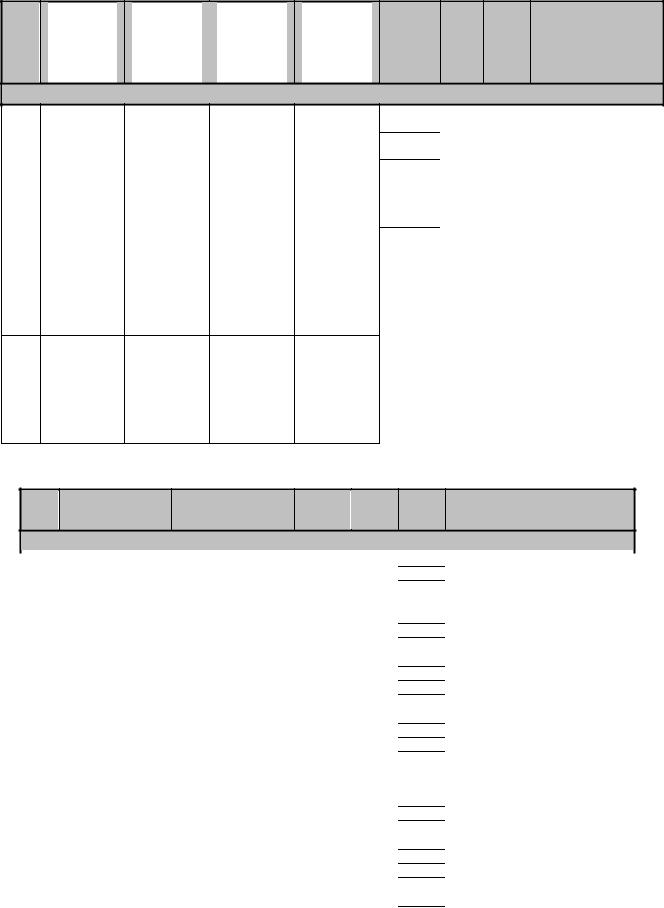
No. |
Function 1 |
Function 2 |
Function 3 |
Function 4 |
IO |
Pull |
PIN |
Comment |
|
LBU |
PHY Debug |
ETM Trace |
|
(Reset |
- |
No. |
|
|
|
and |
and |
|
See |
|
|
|
|
|
GPIO[44:32] |
GPIO[44:32] |
Reserved |
Config |
|
|
|
|
Config |
Config |
Config |
|
[6,5,2]) |
|
|
|
|
(6,5,2)=xx0b |
(6,5,2)=011b |
(6,5,2)=101b |
[6,5,2]=111b |
|
|
|
|
LBU / MII-Interface
166 |
LBU_D12 |
SMI_MDC |
|
|
|
|
|
167 |
LBU_D13 |
SMI_MDIO |
|
|
|
|
|
168 |
LBU_D14 |
RES_PHY_N |
|
|
|
|
|
169 |
LBU_D15 |
GPIO41 |
GPIO41 |
|
|
|
|
170 |
LBU_RDY_N |
GPIO42 |
GPIO42 |
171 |
LBU_IRQ0_N |
GPIO43 |
GPIO43 |
|
|
|
|
172 |
LBU_IRQ1_N |
GPIO44 |
GPIO44 |
B/O/I/O |
up |
W14 |
LBU or MII |
(LBU : I) |
|
|
|
B/O/I/O |
up |
V15 |
LBU or MII |
(LBU : I) |
|
|
|
B/O/I/O |
up |
V16 |
LBU or MII |
(LBU : I) |
|
|
|
B/B/B/B |
up |
W16 |
LBU or GPIO |
(GPIO:I) |
|
|
|
(LBU : I) |
|
|
|
O/B/B/B |
up |
W19 |
LBU or GPIO |
(GPIO:I) |
|
|
LBU-Mode: |
|
|
|
LBU_RDY signal: |
|
|
|
Polarity depends on |
|
|
|
Input CONFIG[6]; |
|
|
|
Output active while |
|
|
|
LBU_CS_R/M_N is |
O/B/B/B |
|
|
active |
up |
AA21 |
LBU or GPIO |
|
(GPIO:I) |
|
|
LBU-Mode: Low-active |
|
|
|
interrupt (no open |
O/B/B/B |
|
|
drain) |
up |
W18 |
LBU or GPIO |
|
(GPIO:I) |
|
|
LBU-Mode: Low-active |
|
|
|
interrupt (no open |
|
|
|
drain) |
1.5.8Ethernet PHY1 and PHY2
No. |
Signal Name |
I/O |
Pull- |
PIN |
Comment |
|
|
|
|
No. |
|
|
|
PHY1 and PHY2 |
|
|
|
173 |
DGND4 |
|
I |
|
T17 |
Digital GND supply |
174 |
DVDD4 |
|
I |
|
R21 |
Digital 1.5 V supply |
175 |
DVDD3 |
|
I |
|
R22 |
Digital 1.5 V supply |
176 |
DGND3 |
|
I |
|
R17 |
Digital GND supply |
177 |
P2VDDARXTX |
|
I |
|
N18 |
Analog Port Tx/Rx 1.5 V supply |
178 |
P2VSSARX |
|
I |
|
N17 |
Analog port GND supply |
179 |
P2RxN |
|
B |
|
P22 |
Port2 differential receive input |
180 |
P2RxP |
|
B |
|
P21 |
Port2 differential receive input |
181 |
P2VSSATX1 |
|
I |
|
M18 |
Analog port GND supply |
182 |
P2TxN |
|
B |
|
M21 |
Port2 differential transmit output |
183 |
P2TxP |
|
B |
|
M22 |
Port2 differential transmit output |
184 |
P2VSSATX2 |
|
I |
|
L19 |
Analog port GND supply |
185 |
P2RDxP |
|
I |
|
U22 |
Port2 FX differential receive input |
186 |
P2RDxN |
|
I |
|
U21 |
Port2 FX differential receive input |
187 |
P2TDxP |
|
O |
|
Y21 |
Port2 FX differential transmit |
|
|
|
|
|
W21 |
output |
188 |
P2TDxN |
|
O |
|
Port2 FX differential transmit |
|
|
|
|
|
|
V19 |
output |
189 |
P2SDxP |
|
I |
|
Port2 FX differential SD input |
|
190 |
P2SDxN |
|
I |
|
U18 |
Port2 FX differential SD input |
191 |
VSSAPLLCB |
|
I |
|
L18 |
Analog central GND supply |
192 |
VDDACB |
|
I |
|
H22 |
Analog central 3.3 V supply |
193 |
VDDAPLL |
|
I |
|
K19 |
Analog central 1.5 V supply |
194 |
EXTRES |
|
B |
|
L21 |
Resistor reference 12.4 kOhm |
195 |
ATP |
|
B |
|
L22 |
Analog test function |
Copyright © Siemens AG 2007. All rights reserved. |
18 |
ERTEC 200 Manual |
Technical data subject to change |
|
Version 1.1.0 |
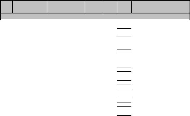
No. |
Signal Name |
I/O |
Pull- |
PIN |
Comment |
|
|
|
|
No. |
|
PHY1 and PHY2 |
|
|
|
|
|
196 |
P1SDxN |
|
I |
|
F19 |
Port1 FX differential SD input |
197 |
P1SDxP |
|
I |
|
G19 |
Port1 FX differential SD input |
198 |
P1TDxN |
|
O |
|
C22 |
Port1 FX differential transmit |
|
|
|
|
|
C21 |
output |
199 |
P1TDxP |
|
O |
|
Port1 FX differential transmit |
|
|
|
|
|
|
E21 |
output |
200 |
P1RDxN |
|
I |
|
Port1 FX differential receive input |
|
201 |
P1RDxP |
|
I |
|
E22 |
Port1 FX differential receive input |
202 |
P1VSSATX2 |
|
I |
|
K18 |
Analog port GND supply |
203 |
P1TxP |
|
B |
|
J22 |
Port1 differential transmit output |
204 |
P1TxN |
|
B |
|
J21 |
Port1 differential transmit output |
205 |
P1VSSATX1 |
|
I |
|
K17 |
Analog port GND supply |
206 |
P1RxP |
|
B |
|
G21 |
Port1 differential receive input |
207 |
P1RxN |
|
B |
|
G22 |
Port1 differential receive input |
208 |
P1VSSARX |
|
I |
|
J17 |
Analog port GND supply |
209 |
P1VDDARXTX |
|
I |
|
J19 |
Analog Port Tx/Rx 1.5 V supply |
210 |
GND33ESD |
|
I |
|
H18 |
Analog test GND supply |
211 |
VDD33ESD |
|
I |
|
F22 |
Analog test 3.3 V supply |
212 |
DGND2 |
|
I |
|
G17 |
Digital GND supply |
213 |
DVDD2 |
|
I |
|
H19 |
Digital 1.5 V supply |
214 |
DVDD1 |
|
I |
|
G18 |
Digital 1.5 V supply |
215 |
DGND1 |
|
I |
|
H21 |
Digital GND supply |
1.5.9Power Supply
No. |
Voltage |
I/O |
PIN No. |
|
Comment |
|
|
Signal Name |
|
|
|
|
|
|
|
|
|
|
|
|
|
|
|
Power Supply |
|
|
|
|
|
|
|
|
|
|
216 |
PLL_AVDD |
P |
E12 |
|
PLL analog, 1.5 V |
|
217 |
PLL_AGND |
P |
F13 |
|
PLL analog GND |
|
218-238 |
VDD Core |
P |
D6, D9, D12, D18, E5, E13, E18, F6, |
|
SV Core 1.5 V |
(21 pins) |
|
|
|
F17, L4, R2, T21, U6, U8, U17, V4, V5, |
|
|
|
|
|
|
V18, W13, W17, AA15 |
|
|
|
239253 |
GND Core |
P |
A21, E6, E11, E17, F5, F7, F16, G6, L5, |
|
GND CORE |
(15 pins) |
|
|
|
T6, U16, V6, V11, V14, AA22 |
|
|
|
254-267 |
VDD IO |
P |
A2, A9, A10, A14, A18, B22, H1, N1, |
|
SV IO 3.3 V |
(14 pins) |
|
|
|
W22, Y1, Y22, AB9, AB15, AB20 |
|
|
|
268-281 |
GND IO |
P |
A8, A12, A20, B1, B21, E10, F8, F15, |
|
GND IO |
(14 pins) |
|
|
|
J1, T1, U5, U7, U15, V17 |
|
|
|
282-285 |
VDDQ (PECL) |
P |
D21, D22, R19, V21 |
|
SV Q PECL 3.3 V |
(4 pins) |
286-288 |
GND (PECL) |
P |
F18, T18, T19 |
|
GND IO (PCI) |
(3 Pins) |
289-304 |
Not Used Pins |
|
E19, F21, H17, J18, K21, K22, |
|
Not Used Pins |
(16 Pins) |
|
|
|
M19, N19, N21, N22, P17, P18, |
|
For improved heat dissipation |
|
|
|
|
P19, R18, T22, V22 |
|
||
|
|
|
|
|
connect these pint to GND. |
|
|
|
|
|
|
However, these pins can also |
|
|
|
|
|
|
remain unconnected. |
|
Table 1: ERTEC 200 Pin Assignment and Signal Description |
|
|
|
|||
Copyright © Siemens AG 2007. All rights reserved. |
19 |
ERTEC 200 Manual |
Technical data subject to change |
|
Version 1.1.0 |

Signal description:
|
IO = |
Signal direction from perspective of the application |
||||
I: |
Input |
|
O: |
Output |
|
|
B: |
Bidirectional |
P: |
Power supply |
|||
|
|
|
|
|||
|
Pull- |
= Internal pull-up/pull-down resistor connected to the signal pin |
||||
up: |
Internal pull-up |
dn: |
Internal pull-down |
|||
|
|
|
||||
|
PU/PD = External resistances necessary, depending on |
|||||
|
application |
|
|
|
|
|
PU: |
External pull-up |
|
PD: |
External pull-down |
||
_N in last position of signal name signifies: Signal is Low active Example: INTA_N
Note:
(1)The BOOT[3:0] pins are read into the “BOOT_REG” system configuration register during the active RESET phase. After a reset, these pins are available as normal function pins.
(2)The CONFIG [6:1] pins are read into the “CONFIG_REG” system configuration register during the active RESET phase. After a reset, these pins are available as normal function pins.
(3)The TMC1 and TMC2 test pins are shorted to ground during operation. TEST_N and TACT_N can remain open.
(4)The GPIOs[31:0] and LBU pins can contain up to 4 different functions. The IO function pins have a different circuitry, corresponding to the selected function.
Example of IO Function: B/O/O/I/ (I) Æ Function 0 = Bidirectional, Function 1 = Output, Function 2 = Output,
Function 3 = Input, (I) = IO Function during RESET = Input
For LBU, PHY-Debug or ETM-Trace-Interface the IO - function is active during Reset, which is selected with the pins CONFIG[6,5,2]. Default the Function 3 (ETM-Trace, GPIO[44:32]) is set with internal Pullupand Pulldown-resistors.
Unusual feature:
ETM-outputs are switched to inputs during Reset. They are changed to outputs after the Trace-Modul is switched on with the debug-module.
Different LBUand GPIO-Pins have bidirectional functions. The value in the bracket is the default value during Reset, if they are selected with CONFIG[6,5,2].
Example:
CONFIG[6, 5, 2] = xx0 Æ Function 1 Æ LBU-Mode
All IO-Pins for Function1 are active during Reset
e.g. |
LBU_A0 is input |
Æ |
Input during Reset |
|
LBU_D0 is bidirectional |
Æ |
Input during Reset |
The alternative GPIO functions are selected by assigning parameters for the GPIO_PORT_MODE_L and
GPIO_PORT_MODE_H registers.
The tabs are described in Section 4.2.2.
The alternative LBU/MII functions are selected with the configuration pins CONFIG[6,5,2] in the user design.
Copyright © Siemens AG 2007. All rights reserved. |
20 |
ERTEC 200 Manual |
Technical data subject to change |
|
Version 1.1.0 |
2 ARM946E-S Processor
The ARM946E-S processor is implemented in the ERTEC 200.
This description is based on /1/ and /2/.
2.1Structure of ARM946E-S
An ARM946E-S processor system is used. The figure below shows the structure of the processor. In addition to the processor core, the system contains one data cache, one instruction cache, a memory protection unit (MPU), a system control coprocessor, and a tightly coupled memory. The processor system has an interface to the integrated AHB bus.
Figure 3: Structure of ARM946E-S Processor System
Copyright © Siemens AG 2007. All rights reserved. |
21 |
ERTEC 200 Manual |
Technical data subject to change |
|
Version 1.1.0 |

2.2Description of ARM946E-S
The ARM946E-S processor system is a member of the ARM9 Thumb family. It has a processor core with Harvard architecture. Compared to the standard ARM9 family, the ARM946E-S has an enhanced V5TE architecture permitting faster switching between ARM and Thumb code segments and an enhanced multiplier structure. In addition, the processor has an integrated JTAG interface.
2.3Operating Frequency of ARM946E-S
The processor can be operated at 50 MHz, 100 MHz, or 150 MHz. The operating frequency is set during the reset phase via the configuration pins CONFIG[4] and CONFIG[3]. Communication with the components of the ERTEC 200 takes place via the AHB bus at a frequency of 50 MHz.
2.4Cache Structure of ARM946E-S
The following caches are integrated in the ARM946E-S.
•8 Kbytes of instruction cache with lock function
•4 Kbytes of data cache with lock function
Both caches are “Four-Way Set Associative” caches with 1-Kbyte segments. Each segment consists of 32 lines with 32 bytes (8 x 4 bytes). The D-cache has “write buffers" with write-back function.
The lock function enables the user to lock (LOCK) the contents of the cache segments. This function enables the command set for fast routines to be maintained permanently in the instruction cache. This mechanism can only be applied at the segment level with the ARM946E-S.
Both caches are locked after a reset. These caches can only be enabled if the Memory Protection Unit is also enabled. The I-cache can be enabled by setting Bit 12 of the CP15 control register.
The D-cache can be enabled by setting Bit 2 of the CP15 control register. Access to this area is blocked if the cache is not enabled.
For additional information about Caching refer to Document /1/ Section 3.
For more information on the description of the ARM946 registers, refer to Section 2.10 of this document.
2.5Tightly Coupled Memory (TCM)
A 4-Kbyte data-tightly coupled memory (D-TCM) is implemented in the ARM946E-S processor of the ERTEC 200. The memory is locked after a reset. The D-TCM can be placed in the address area of the ARM946E-S as desired and must be used together with a region of the memory protection unit. Data from high-speed routines such as isochronous control can be placed in the D-TCM.
The D-TCM can be enabled by setting Bit 16 of the CP15 control register.
In addition, the address area of the D-TCM must be set in the Tightly-Coupled Memory register.
For more information about the D-TCM refer to document /1/ Section 5.
For more information on the description of the ARM946 registers, refer to Section 2.10 of this document.
Copyright © Siemens AG 2007. All rights reserved. |
22 |
ERTEC 200 Manual |
Technical data subject to change |
|
Version 1.1.0 |

2.6Memory Protection Unit (MPU)
The memory protection unit enables the user to partition specific memory areas (I-cache, D-cache, or DTCM) into various regions and to assign different attributes to them.
A maximum of 8 regions of variable size can be set. If regions overlap, the attributes of the higher region number apply. Settings for each region:
•Base address of region
•Size of region
•Cache and “write buffer” configuration
•Read/write access enable for privileged users/users
Settings are made in the following registers of the ARM946E-S:
Register 2 “Cache configuration register”
Register 3 “Write buffer control register”
Register 5 “Access permission register”
Register 6 “Protection region/base size register”
The base address defines the start address of the region. It must always be a multiple of the size of the region. Example: The region size is 4 Kbytes. The starting address is then always a multiple of 4 Kbytes.
Before the MPU is enabled, at least one region must have been assigned. Otherwise, the ARM946E-S can assume a state that can only be cancelled by a reset.
The MPU can be enabled by setting Bit 0 of the CP15 control register.
If the MPU is disabled, the I-cache- and D-cache cannot be accessed, even if they are enabled.
For more information about the MPU refer to Document /1/ Section 4.
For more information on the description of the ARM946 registers, refer to Section 2.10 of this document.
2.7Bus Interface of ARM946E-S
The ARM946E-S uses an AHB bus master interface to the multilayer AHB bus for opcode fetches and data transfers. The interface operates at a fixed frequency of 50 MHz. The data bus and address bus each have a width of 32 bits.
For more information about the bus interface and write buffer, and about the different transfer types, refer to Document
/1/ Section 6.
2.8ARM946E-S Embedded Trace Macrocell (ETM9)
An ETM9 module is connected at the ARM946E-S. This module permits debugging support for data and instruction traces in the ERTEC 200. The module contains all signals required by the processor for the data and instruction traces. The ETM9 module is operated by means of the JTAG interface. The trace information is provided outwards to the trace port via a FIFO memory. A detailed description can be found in Section 11
2.9ARM Interrupt Controller (ICU)
The interrupt controller supports the FIQ and IRQ interrupt levels of the ARM946 processor. An interrupt controller with 8 interrupt inputs is implemented for FIQ. Six interrupt inputs (FIQ0-5) are occupied by the ERTEC 200, and 2 interrupt inputs (FIQ6-7) can be programmed optionally as IRQ sources. The high-priority FIQ interrupts are used for watchdog and address area monitoring and for debugging. An interrupt controller for 16 interrupt inputs is implemented for IRQ. Of the 16 IRQ inputs, two IRQ sources can be selected for as Fast-Interrupt_Requests (FIQ6-7) for processing. The assignment is made by specifying the IRQ number of the relevant interrupt input in the FIQ1REG / FIQ2REG register. The interrupt inputs selected as FIQ must be disabled for the IRQ logic. All other interrupt inputs can continue to be processed as IRQs.
The interrupt controller is operated at a clock frequency of 50 MHz. Interrupt-request signals generated with a higher frequency must be lengthened accordingly for error-free detection.
Copyright © Siemens AG 2007. All rights reserved. |
23 |
ERTEC 200 Manual |
Technical data subject to change |
|
Version 1.1.0 |

2.9.1Prioritization of Interrupts
It is possible to set the priorities of the IRQ and FIQ interrupts. Priorities 0 to 15 can be assigned to IRQ interrupts while priorities 0 to 7 can be assigned to FIQ interrupts. The highest priority is 0 for both interrupt levels. After a reset, all IRQ interrupt inputs are set to priority 15 and all FIQ interrupt inputs are set to priority 7. A priority register is associated with each interrupt input. PRIOREG0 to PRIOREG15 are for the IRQ interrupts and FIQPR0 to FIQPR7 are for the FIQ interrupts. A priority must not be assigned more than once. A check for the assignment of identical priorities is not performed in the ICU logic. All interrupt requests with a lower or equal priority can be blocked at any time in the IRQ priority resolver by assigning a priority in the LOCKREG register. If an interrupt that is to be blocked is requested at the same time as the write access to the LOCKREG register, an IRQ signal is output. However, the signal is revoked after two clock cycles. If an acknowledgement is to be generated nonetheless, the transferred interrupt vector is the default vector.
2.9.2Trigger Modes
The “Edge-triggered” and “Level-triggered” operating modes are available for each interrupt input.
The trigger type is defined by means of the assigned bit in the TRIGREG register. For the “Edge-triggered” mode setting, differentiation can be made between a positive and negative edge evaluation. This is made in the EDGEREG register. In “Level-triggered” mode, the active level of the interrupt request is high active. By default, the IRQ interrupt parameters are assigned as described in Section 2.9.7, and the FIQ interrupts parameters are assigned as described in Section 2.9.8.
In “Edge-triggered” mode, the interrupt input signal must be present for at least one clock cycle. In “Level-triggered” mode, the input signal must be present until the ARM946E-S CPU is confirmed. Shorter signals result in loss of the event.
2.9.3Masking the Interrupt Inputs
Each IRQ interrupt can be enabled or disabled individually. The MASKREG register is available for this purpose. The interrupt mask acts only after the IRREG interrupt request register. That is, an interrupt is entered in the IRREG register in spite of the block in the MASKREG register. After a reset, all mask bits are set and, thus, all interrupts are disabled. At a higher level, all IRQ interrupts can be disabled globally via a command. When IRQ interrupts are enabled globally via a command, only those IRQ interrupts that are enabled by the corresponding mask bit in the MASKREG register are enabled.
For the FIQ interrupts, only selective masking by the mask bits in the FIQ_MASKREG register is possible. After a reset, all FIQ interrupts are disabled. A detected FIQ interrupt request is entered in the FIQ interrupt request register. If the interrupt is enabled in the mask register, processing takes place in the priority logic. If the interrupt request is accepted by the ARM946 CPU and an entry is made in the in-service request register (ISR), the corresponding bit is reset in the IRREG register. Each bit that is set in the IRREG register can be deleted via software. For this purpose, the number of the bit to be reset in the IRCLVEC register is transferred to the interrupt controller.
2.9.4Software Interrupts for IRQ
Every IRQ interrupt request can be triggered by setting the bit corresponding to the input channel in the software interrupt register SWIRREG. Multiple requests can also be entered in the 16-bit SWIRREG register. The software interrupt requests are received directly in the IRREG register and, thus, treated like a hardware IRQ. Software interrupts can only be triggered by the ARM946E-S processor because only it has access authorization to the interrupt controller.
2.9.5Nested Interrupt Structure
When enabled by the interrupt priority logic, an IRQ interrupt request causes an IRQ signal to be output. Similarly, an FIQ interrupt request causes the FIQ signal to be output to the CPU.
When the request is accepted by the CPU, the bit corresponding to the physical input in the register ISRREG is set. The IRQ/FIQ signal is revoked. The ISR bit of the accepted interrupt remains set until the CPU returns an End-Of-Interrupt command to the interrupt controller. As long as the ISR bit is set, interrupts with lower priority in the priority logic of the interrupt controller are disabled. Interrupts with a higher priority are allowed by the priority logic to pass and generate an IRQ/FIQ signal to the CPU. As soon as the CPU accepts this interrupt, the corresponding ISR bit in the ISRREG register is also set. The CPU then interrupts the lower-priority interrupt routine and executes the higher interrupt routine first. Lower-priority interrupts are not lost. They are entered in the IRREG register and are processed at a later time when all higher-priority interrupt routines have been executed.
2.9.6EOI End-Of-Interrupt
A set ISR bit is reset by the End-Of-Interrupt command. The CPU must communicate this to the interrupt controller with the EOI command after processing of the corresponding interrupt server routine. To communicate the EOI command to the interrupt controller, the CPU writes any value to the IRQEND/FIQEND registers. The interrupt controller decides independently which ISR bit will be reset with the EOI command. If several ISR bits are set, the interrupt controller deletes the ISR bit of the highest-priority interrupt request at the time of the EOI command. The interrupt cycle is considered complete for the interrupt controller when all set ISR bits have been reset by the corresponding number of EOI commands. After this, lower-priority interrupts that have occurred in the meantime and have been entered in the RREG register can be processed in the priority logic.
During one or more accepted interrupts, the priority distribution of the IRQ/FIQ interrupt inputs must not be changed because the ICU can otherwise no longer correctly assign the EOI commands.
Copyright © Siemens AG 2007. All rights reserved. |
24 |
ERTEC 200 Manual |
Technical data subject to change |
|
Version 1.1.0 |

The CPU accepts an IRQ-/FIQ request by reading the IRVEC/FIVEQ register. This register contains the binary-coded vector number of the highest priority interrupt request at the moment. Each of the two interrupt vector registers can be referenced using two different addresses. The interrupt controller interprets the reading of the vector register with the first address as an “interrupt acknowledge”. This causes the sequences for this interrupt to be implemented in the ICU logic. Reading of the vector register with the second address is not linked to the “acknowledge function”. This is primarily useful for the debugging functions in order to read out the content of the interrupt vector register without starting the acknowledge function of the interrupt controller.
2.9.7IRQ Interrupt Sources
Interrupts from the following function groups of the ERTEC 200 are available to the IRQ interrupt controller:
IRQ Interrupts
Interrupt-Nr. |
Function Block |
Signal Name |
Default Setting |
Comment |
|
0 |
Timer |
TIM_INT0 |
Rising edge |
Timer 0 |
|
|
|
|
|
|
|
1 |
Timer |
TIM_INT1 |
Rising edge |
Timer 1 |
|
3:2 |
GPIO |
GPIO (1:0) |
Assignable |
External input ERTEC 200 GPIO[1:0] |
|
|
|
|
|
|
|
5:4 |
GPIO |
GPIO (31:30) |
Assignable |
External input ERTEC 200 |
|
GPIO[31:30] |
|||||
|
|
|
|
||
6 |
Timer |
TIM_INT2 |
Rising edge |
Timer 2 |
|
|
|
|
|
|
|
7 |
----- |
------ |
----- |
Reserved |
|
|
|
|
|
|
|
8 |
UART |
UART_INTR |
High level |
Group interrupt UART |
|
|
|
|
|
|
|
9 |
PHY0/1 |
P0/1_INTERP |
Rising edge |
Interrupt von PHY 0/1 |
|
10 |
SPI |
SSP_INTR |
Rising edge |
Group interrupt SPI |
|
11 |
SPI |
SSP_ROR_INTR |
Rising edge |
Receive overrun interrupt SPI |
|
|
|
|
|
|
|
12 |
IRT switch |
IRQ0_SP |
Rising edge |
High-priority IRT interrupt |
|
|
|
|
|
|
|
13 |
IRT switch |
IRQ1_SP |
Rising edge |
Low-priority IRT interrupt |
|
14 |
----- |
----- |
----- |
Reserved |
|
15 |
DMA |
DMA_INT |
Rising edge |
DMA controller, DMA transfer |
|
complete |
|||||
|
|
|
|
||
Table 2: Overview of IRQ Interrupts |
|
|
|
||
2.9.8FIQ Interrupt Sources
Interrupts from the following function groups of the ERTEC 200 are available to the FIQ interrupt controller:
FIQ Interrupts
Interrupt-Nr. |
Function Block |
Signal Name |
Default Setting |
Comment |
|
0 |
Watchdog |
|
Rising edge |
|
|
1 |
APB bus |
|
Rising edge |
Access to non-existing address at |
|
|
the APB (1) |
||||
|
|
|
|
||
2 |
Multilayer AHB |
|
Rising edge |
Access to non-existing address at |
|
|
the AHB (1) |
||||
|
|
|
|
||
|
|
|
|
Group interrupt of: |
|
|
|
|
|
EMIF: I/O time-out |
|
3 |
PLL-Status-Register |
|
Rising edge |
PLL: Loss state |
|
|
PLL: Lock State |
|
|||
|
|
|
|
|
|
|
|
|
|
see system control register |
|
|
|
|
|
"PLL_STAT_REG" |
|
4 |
ARM-CPU |
COMM_Rx |
Rising edge |
Receive comm channel interrupt |
|
5 |
ARM-CPU |
COMM_Tx |
Rising edge |
Transmit comm channel interrupt |
|
6 |
Optional |
Optional from IRQ |
Rising edge |
User-programmable IRQ source |
|
7 |
Optional |
Optional from IRQ |
Rising edge |
User-programmable IRQ source |
|
Table 3: Overview of FIQ Interrupts
(1)Access to non-existing addresses is detected by the individual function groups of the ERTEC 200 and triggers a pulse with duration Tp = 2/50 MHz. For evaluation of this interrupt, the connected FIQ input must be specified as an edge-triggered input.
Copyright © Siemens AG 2007. All rights reserved. |
25 |
ERTEC 200 Manual |
Technical data subject to change |
|
Version 1.1.0 |

2.9.9IRQ Interrupts as FIQ Interrupt Sources
Interrupts from the IRQ interrupt can be placed on FIQ6 and FIQ7 können.
The interrupts of the FIQ interrupt controller are used for debugging, monitoring address area access, and for the watchdog.
FIQ interrupts no. 4 and 5 are the interrupts for embedded ICE RT communication. The UART can also be used as a debugger in place of the ICE. Effective real-time debugging is possible when the IRQ interrupt sources of the UART are mapped to the FIQs with the number 6 or 7. This enables debugging of interrupt routines.
2.9.10 Interrupt Control Register
The interrupt control registers are used to specify all aspects of control, prioritization, and masking of the IRQ/FIQ interrupt controllers.
|
|
ICU (Base Address 0x5000_0000) |
|
|
||||
|
|
|
|
|||||
Register Name |
Offset Address |
Address Area |
|
|
Access |
Default |
Description |
|
IRVEC |
0x0000 |
4 bytes |
|
|
R |
0xFFFFFFFF |
Interrupt vector register |
|
FIVEC |
0x0004 |
4 bytes |
|
|
R |
0xFFFFFFFF |
Fast interrupt vector register |
|
LOCKREG |
0x0008 |
4 bytes |
|
|
R/W |
0x00000000 |
Priority lock register |
|
FIQ1SREG |
0x000C |
4 bytes |
|
|
R/W |
0x00000000 |
Fast int. request 1 select register |
|
|
|
(FIQ6 on FIQ interrupt controller) |
|
|||||
|
|
|
|
|
|
|
|
|
FIQ2SREG |
0x0010 |
4 bytes |
|
|
R/W |
0x00000000 |
Fast int. request 2 select register |
|
|
|
(FIQ7 on FIQ interrupt controller) |
|
|||||
|
|
|
|
|
|
|
|
|
IRQACK |
0x0014 |
4 bytes |
|
|
R |
0xFFFFFFFF |
Interrupt vector register with IRQ |
|
|
|
|
|
|
|
|
acknowledge |
|
FIQACK |
0x0018 |
4 bytes |
|
|
R |
0xFFFFFFFF |
Fast interrupt vector register with |
|
|
|
|
|
|
|
|
FIQ acknowledge |
|
IRCLVEC |
0x001C |
4 bytes |
|
|
W |
0x---- |
Interrupt request clear vector |
|
MASKALL |
0x0020 |
4 bytes |
|
|
R/W |
0x00000001 |
Mask for all interrupts |
|
IRQEND |
0x0024 |
4 bytes |
|
|
W |
0x---- |
End of IRQ interrupt |
|
FIQEND |
0x0028 |
4 bytes |
|
|
W |
0x---- |
End of FIQ interrupt |
|
FIQPR0 |
0x002C |
4 bytes |
|
|
R/W |
0x00000007 |
FIQ priority register on input FIQ0 |
|
|
|
|
|
|
|
|
of the FIQ interrupt controller |
|
FIQPR1 |
0x0030 |
4 bytes |
|
|
R/W |
0x00000007 |
FIQ priority register on input FIQ1 |
|
|
|
|
|
|
|
|
of the FIQ interrupt controller |
|
FIQPR2 |
0x0034 |
4 bytes |
|
|
R/W |
0x00000007 |
FIQ priority register on input FIQ2 |
|
|
|
|
|
|
|
|
of the FIQ interrupt controller |
|
FIQPR3 |
0x0038 |
4 bytes |
|
|
R/W |
0x00000007 |
FIQ priority register on input FIQ3 |
|
|
|
|
|
|
|
|
of the FIQ interrupt controller |
|
FIQPR4 |
0x003C |
4 bytes |
|
|
R/W |
0x00000007 |
FIQ priority register on input FIQ4 |
|
|
|
|
|
|
|
|
of the FIQ interrupt controller |
|
FIQPR5 |
0x0040 |
4 bytes |
|
|
R/W |
0x00000007 |
FIQ priority register on input FIQ5 |
|
|
|
|
|
|
|
|
of the FIQ interrupt controller |
|
FIQPR6 |
0x0044 |
4 bytes |
|
|
R/W |
0x00000007 |
FIQ priority register on input FIQ6 |
|
|
|
|
|
|
|
|
of the FIQ interrupt controller |
|
FIQPR7 |
0x0048 |
4 bytes |
|
|
R/W |
0x00000007 |
FIQ priority register on input FIQ7 |
|
|
|
|
|
|
|
|
of the FIQ interrupt controller |
|
FIQISR |
0x004C |
4 bytes |
|
|
R |
0x00000000 |
FIQ in-service register |
|
FIQIRR |
0x0050 |
4 bytes |
|
|
R |
0x00000020 |
FIQ request register |
|
FIQ_MASKREG |
0x0054 |
4 bytes |
|
|
R/W |
0x000000FF |
FIQ interrupt mask register |
|
IRREG |
0x0058 |
4 bytes |
|
|
R |
0x000001xx |
Interrupt request register |
|
MASKREG |
0x005C |
4 bytes |
|
|
R/W |
0x0000FFFF |
Interrupt mask register |
|
ISREG |
0x0060 |
4 bytes |
|
|
R |
0x00000000 |
In-service register |
|
TRIGREG |
0x0064 |
4 bytes |
|
|
R/W |
0x00000000 |
Trigger select register |
|
EDGEREG |
0x0068 |
4 bytes |
|
|
R/W |
0x00000000 |
Edge select register |
|
SWIRREG |
0x006C |
4 bytes |
|
|
R/W |
0x00000000 |
Software interrupt register |
|
PRIOREG 0 |
0x0070 |
4 bytes |
|
|
R/W |
0x0000000F |
Priority register 0 |
|
|
|
|
|
|
||||
Copyright © Siemens AG 2007. All rights reserved. |
26 |
|
|
ERTEC 200 Manual |
||||
Technical data subject to change |
|
|
|
|
|
Version 1.1.0 |
||

|
PRIOREG 1 |
|
0x0074 |
|
4 bytes |
|
R/W |
|
0x0000000F |
|
.... |
|
|
|
|
|
|
|
|
||||||
|
... |
|
... |
|
|
|
|
|
|
|
.... |
|
|
... |
|
... |
|
|
|
|
|
|
|
.... |
|
|
PRIOREG15 |
|
0x00AC |
|
4 bytes |
|
R/W |
|
0x0000000F |
|
Priority register 15 |
|
|
Table 4: Overview of Interrupt Control Register |
|
|
|
|
|
|
|
|
|||
|
2.9.11 ICU Register Description |
|
|
|
|
|
|
|
|
|||
IRVEC |
|
R |
|
Addr.: 0x5000_0000 |
Default: 0xFFFF_FFFF |
|
Description |
|
Interrupt vector register |
|
|
||
|
|
|
Input with highest priority pending interrupt request |
|
||
|
|
|
|
|
|
|
Bit No. |
|
Name |
|
Description |
|
|
3:0 |
|
IRVEC |
For pending, valid interrupt: Binary code of input number. |
|||
|
|
|
|
Default vector: Bit[3:0] = 1 |
|
|
31:4 |
|
Vector ID |
For pending, valid interrupt: Bit[31:4] = 0. |
|
||
|
|
|
|
Default vector: Bit[31:4] = 1 |
|
|
|
|
|
|
|
|
|
FIVEC |
|
R |
|
Addr.: 0x5000_0004 |
Default: 0xFFFF_FFFF |
|
Description |
|
Fast interrupt vector register |
|
|
||
|
|
|
Number of the highest-priority pending fast interrupt request |
|
||
|
|
|
|
|
|
|
Bit No. |
|
Name |
|
Description |
|
|
2:0 |
|
FIVEC |
For pending, valid interrupt: Binary code of FIQ number. |
|||
|
|
|
|
Default vector: Bit[2:0] = 1 |
|
|
31:3 |
|
Vector ID |
For pending valid Bit[31:3] = 0. |
|
||
|
|
|
|
Default vector: Bit[31:3] = 1 |
|
|
|
|
|
|
|
||
LOCKREG |
|
R/W |
Addr.: 0x5000_0008 |
Default: 0x0000_0000 |
||
Description |
|
Priority lock register |
|
|
||
|
|
|
Specification of a priority for blocking interrupt requests of lower and equal priority |
|||
|
|
|
|
|
|
|
Bit No. |
|
Name |
|
Description |
|
|
3 – 0 |
|
LOCKPRIO |
Binary code of lock priority. |
|
||
7 |
|
LOCKENABLE |
0=Lock inactive / 1=Lock active |
|
||
|
|
|
|
|
||
FIQ1SREG |
|
R/W |
Addr.: 0x5000_000C |
Default: 0x0000_0000 |
||
Description |
|
Fast interrupt request 1 select register |
|
|||
|
|
|
Declaration of an IRQ input as FIQ6 (input FIQ6 on FIQ interrupt controller) |
|||
|
|
|
|
|
|
|
Bit No. |
|
Name |
|
Description |
|
|
3 – 0 |
|
FIQ1SREG |
Number of the input to be selected (binary code) |
|||
7 |
|
FIQ1SENABLE |
0=Ignore FIQ declaration |
|
||
|
|
|
|
0=Take into account FIQ declaration |
|
|
|
|
|
|
|
||
FIQ2SREG |
|
R/W |
Addr.: 0x5000_0010 |
Default: 0x0000_0000 |
||
Description |
|
Fast interrupt request 2 select register |
|
|||
|
|
|
Declaration of an IRQ input as FIQ7 (input FIQ7 on FIQ interrupt controller) |
|||
|
|
|
|
|
|
|
Bit No. |
|
Name |
|
Description |
|
|
3 – 0 |
|
FIQ2SREG |
Number of the input to be selected (binary code) |
|||
7 |
|
FIQ2SENABLE |
0=Ignore FIQ declaration |
|
||
|
|
|
|
0=Take into account FIQ declaration |
|
|
|
|
|
|
|
|
|
IRQACK |
|
R |
|
Addr.: 0x5000_0014 |
Default: 0xFFFF_FFFF |
|
Description |
|
Interrupt vector register with IRQ acknowledge |
|
|||
|
|
|
Confirmation of highest-priority pending interrupt request by reading |
|||
|
|
|
the associated interrupt vector |
|
|
|
Bit No. |
|
Name |
|
Description |
|
|
3 – 0 |
|
IRVEC |
Binary code of input number |
|
||
31 - 4 |
|
Vector ID |
Valid IRQ vector: always ‘0’. |
|
||
|
|
|
|
Default vector: always ‘1’ (also bits 3 – 0). |
|
|
Copyright © Siemens AG 2007. All rights reserved. |
27 |
ERTEC 200 Manual |
Technical data subject to change |
|
Version 1.1.0 |

FIQACK |
|
R |
|
Addr.: 0x5000_0018 |
|
Default: 0xFFFF_FFFF |
|
Description |
|
Fast interrupt vector register with FIQ acknowledge |
|
|
|||
|
|
Confirmation of fast interrupt request by reading the associated |
|
||||
|
|
interrupt vector |
|
|
|
|
|
Bit No. |
Name |
|
|
Description |
|
|
|
2 – 0 |
FIVEC |
|
Binary code of FIQ number |
|
|
||
31 – 3 |
Vector ID |
|
Valid FIQ vector: always ‘1’. |
|
|
||
|
|
|
|
Default vector: always ‘1’ (also bits 2 – 0). |
|
||
|
|
|
|
|
|
||
IRCLVEC |
|
W |
|
Addr.: 0x5000_001C |
Default: ---- |
||
Description |
|
Interrupt request clear vector |
|
|
|
||
|
|
Immediate deletion of an interrupt request in the interrupt request register |
|||||
|
|
|
|
|
|
|
|
Bit No. |
Name |
|
|
Description |
|
|
|
3 – 0 |
IRCLVEC |
|
Binary code of the input number of the request to be deleted |
||||
7 |
unused |
|
|
|
|
|
|
|
|
|
|
|
|
||
MASKALL |
|
R/W |
Addr.: 0x5000_0020 |
|
Default: '1' |
||
Description |
|
Mask all Interrupts |
|
|
|
|
|
|
|
Global disable for all IRQ interrupt inputs |
|
|
|||
|
|
|
|
|
|
|
|
Bit No. |
Name |
|
|
Description |
|
|
|
0 |
MASKALL |
|
'0' = Enable all non-masked IRQ interrupt inputs |
||||
|
|
|
|
(consideration given to set mask bits) |
|
||
|
|
|
|
'1' = Global disable for all IRQ interrupt inputs |
|||
|
|
|
|
(independent of the interrupt mask) |
|
||
|
|
|
|
|
|
|
|
IRQEND |
|
W |
|
Addr.: 0x5000_0024 |
|
Default: ---- |
|
|
|
|
|
|
|
||
Description |
|
End-of-interrupt (IRQ) |
|
|
|
||
|
|
Communicates to the IRQ interrupt controller the completion of the interrupt service routine |
|||||
|
|
associated with the current request |
|
|
|||
Bit No. |
Name |
|
|
Description |
|
|
|
|
Not used |
|
|
|
|
|
|
|
|
|
|
|
|
|
|
FIQEND |
|
W |
|
Addr.: 0x5000_0028 |
|
Default: ---- |
|
Description |
|
End-of-interrupt (FIQ) |
|
|
|
||
|
|
Communicates to the FIQ interrupt controller the completion of the interrupt service routine |
|||||
|
|
associated with the fast interrupt request |
|
|
|||
Bit No. |
Name |
|
|
Description |
|
|
|
|
Not used |
|
|
|
|
|
|
|
|
|
|
|
|
||
FIQPR0 |
|
R/W |
|
Addr.: 0x5000_002C |
Default: 0x0000_0007 |
||
… |
|
…. |
|
Addr.: 0x5000_0048 |
|
Default: 0x0000_0007 |
|
FIQPR7 |
|
R/W |
|
|
|||
Description |
|
FIQ priority registers |
|
|
|
||
|
|
Priority of the fast interrupt request at input FIQ0 to FIQ7 of the FIQ interrupt controller |
|||||
|
|
|
|
|
|
|
|
Bit No. |
Name |
|
|
Description |
|
|
|
2 – 0 |
FIQPR0 to 7 |
|
Binary code of the priority |
|
|
||
7 – 3 |
Not used |
|
|
|
|
|
|
|
|
|
|
|
|||
FIQISR |
|
R |
Addr.: 0x5000_004C |
Default: 0x0000_0000 |
|||
|
|
|
|
|
|
||
Description |
|
FIQ in-service register |
|
|
|
||
|
|
Indication of the fast interrupt requests confirmed by the CPU |
|
||||
|
|
|
|
|
|
|
|
Bit No. |
Name |
|
|
Description |
|
|
|
7 – 0 |
FIQISR |
|
Inputs 0 to 7 of the FIQ interrupt controller |
|
|||
|
|
|
|
'0' = Fast interrupt request not confirmed |
|
||
|
|
|
|
'1' = Fast interrupt request has been confirmed |
|||
Copyright © Siemens AG 2007. All rights reserved. |
28 |
ERTEC 200 Manual |
Technical data subject to change |
|
Version 1.1.0 |

FIQIRR |
|
R |
Addr.: 0x5000_0050 |
Default: 0x0000_0020 |
Description |
|
FIQ request register |
|
|
|
|
Indication of the fast interrupt request detected with a positive edge |
||
|
|
|
|
|
Bit No. |
Name |
|
Description |
|
7 – 0 |
FIQIRR |
Inputs 0 to 7 of the FIQ interrupt controller |
|
|
|
|
|
'0' = No request |
|
|
|
|
'1' = Request is occurred |
|
FIQ_MASKREG |
|
R/W |
Addr.: 0x5000_0054 |
Default: 0x0000_00FF |
|||
Description |
|
|
Interrupt mask register for FIQ |
|
|
||
|
|
|
Enable/disable of FIQ interrupt inputs |
|
|||
|
|
|
|
|
|
|
|
Bit No. |
Name |
|
|
|
Description |
|
|
7 – 0 |
FIQ_MASKREG |
|
FIQ interrupt input 0 to 7 |
|
|||
|
|
|
|
|
0' = Interrupt input enabled |
|
|
|
|
|
|
|
'1' = Interrupt input disabled |
|
|
IRREG |
|
R |
Addr.: 0x5000_0058 |
Default:0x0000_01xx |
Description |
|
Interrupt request register |
|
|
|
|
Storage of interrupt requests that have occurred |
|
|
|
|
|
|
|
Bit No. |
Name |
|
Description |
|
15 – 0 |
IRREG |
Interrupt input 0 to 15 |
|
|
|
|
|
0=Interrupt request inactive/1=Interrupt request active |
|
|
|
|
Bit 5, 4, 3, 2 depending on GPIO 31, 30, 1, 0 |
|
MASKREG |
|
|
R/W |
Addr.: 0x5000_005C |
Default: 0x0000_FFFF |
||
Description |
|
Interrupt mask register |
|
|
|||
|
|
|
Enable/disable of interrupt inputs |
|
|
||
|
|
|
|
|
|
|
|
Bit No. |
|
Name |
|
|
Description |
|
|
15 – 0 |
|
MASKREG |
|
Interrupt input 0 to 15 |
|
||
|
|
|
|
|
0=Interrupt input enabled/1=Interrupt input disabled |
||
ISREG |
|
R |
Addr.: 0x5000_0060 |
Default: 0x0000_0000 |
Description |
|
In-service register |
|
|
|
|
Indication of the interrupt requests confirmed by the CPU |
|
|
|
|
|
|
|
Bit No. |
Name |
|
Description |
|
15 – 0 |
ISREG |
Interrupt input 0 to 15 |
|
|
|
|
|
0=Interrupt request not confirmed |
|
|
|
|
1=Interrupt request has been confirmed |
|
TRIGREG |
|
|
R/W |
Addr.: 0x5000_0064 |
Default: 0x0000_0000 |
|
Description |
|
Trigger select register |
|
|
||
|
|
Selection of interrupt detection |
|
|
||
|
|
|
|
|
|
|
Bit No. |
Name |
|
|
Description |
|
|
15 – 0 |
TRIGREG |
|
Interrupt input 0 to 15 |
|
||
|
|
|
|
0=Interrupt detection via edge |
|
|
|
|
|
|
1=Interrupt detection via level |
|
|
EDGEREG |
|
|
R/W |
Addr.: 0x5000_0068 |
Default: 0x0000_0000 |
||
Description |
|
Edge select register |
|
|
|||
|
|
|
Edge selection for interrupt detection |
|
|||
|
|
|
(only if edge detection is specified for the associated input) |
|
|||
Bit No. |
|
Name |
|
|
Description |
|
|
15 – 0 |
|
EDGEREG |
|
Interrupt input 0 to 15 |
|
||
|
|
|
|
|
0=Interrupt detection via positive edge |
|
|
|
|
|
|
|
1=Interrupt detection via negative edge |
|
|
Copyright © Siemens AG 2007. All rights reserved. |
29 |
ERTEC 200 Manual |
Technical data subject to change |
|
Version 1.1.0 |
SWIRREG |
|
|
R/W |
Addr.: 0x5000_006C |
Default: 0x0000_0000 |
|
Description |
|
Software interrupt register |
|
|
||
|
|
Specification of interrupt requests |
|
|||
|
|
|
|
|
|
|
Bit No. |
Name |
|
|
Description |
|
|
15 – 0 |
SWIRREG |
|
Interrupt input 0 to 15 |
|
||
|
|
|
|
0=No interrupt request |
|
|
|
|
|
|
1=Set interrupt request |
|
|
PRIOREG 0 |
|
R/W |
Addr.: 0x5000_0070 |
Default: 0x0000_000F |
|||
… |
|
|
|
…. |
Addr.: 0x5000_00AC |
Default: 0x0000_000F |
|
PRIOREG 15 |
|
R/W |
|||||
Description |
|
|
Priority register |
|
|
||
|
|
|
Specification of priority of an interrupt request at the associated input |
||||
|
|
|
|
|
|
|
|
Bit No. |
Name |
|
|
|
Description |
|
|
3 – 0 |
PRIOREG |
|
Binary code of the priority |
|
|||
Copyright © Siemens AG 2007. All rights reserved. |
30 |
ERTEC 200 Manual |
Technical data subject to change |
|
Version 1.1.0 |
Loading...