


VPC-X360EX
SERVICE MANUAL
Color Digital Camera
VPC-X360E
VPC-X360EX
(Product Code : 126 251 01)
(U.K.)
(Product Code : 126 251 02)
(Europe)
(PAL General)
Contents
1. OUTLINE OF CIRCUIT DESCRIPTION ....................2
2. DISASSEMBLY........................................................12
3. ELECTRICAL ADJUSTMENT..................................15
4. TROUBLESHOOTING GUIDE.................................20
5. PARTS LIST.............................................................21
CABINET AND CHASSIS PARTS 1 ........................21
CABINET AND CHASSIS PARTS 2 ........................22
ELECTRICAL PARTS .............................................. 23
ACCESSORIES .......................................................28
PACKING MATERIALS............................................28
CIRCUIT DIAGRAM (Refer to the separate volume)
The components designated by a symbol ( ! ) in this schematic diagram designates components whose value are of
special significance to product safety. Should any component designated by a symbol need to be replaced, use only the part
designated in the Parts List. Do not deviate from the resistance, wattage, and voltage ratings shown.
CAUTION : Danger of explosion if battery is incorrectly replaced.
Replace only with the same or equivalent type recommended by the manufacturer.
Discard used batteries according to the manufacturer’s instructions.
NOTE : 1. Parts order must contain model number, part number, and description.
2. Substitute parts may be supplied as the service parts.
3. N. S. P. : Not available as service parts.
Design and specification are subject to change without notice.
SR662/E, EX, U
REFERENCE No. SM5310090
FILE NO.
PRODUCT SAFETY NOTICE
VPC-X360
(Product Code : 126 251 03)
(U.S.A.)
(Canada)
−2−
Pin 1
2
8
34
2
H
V
Pin 9
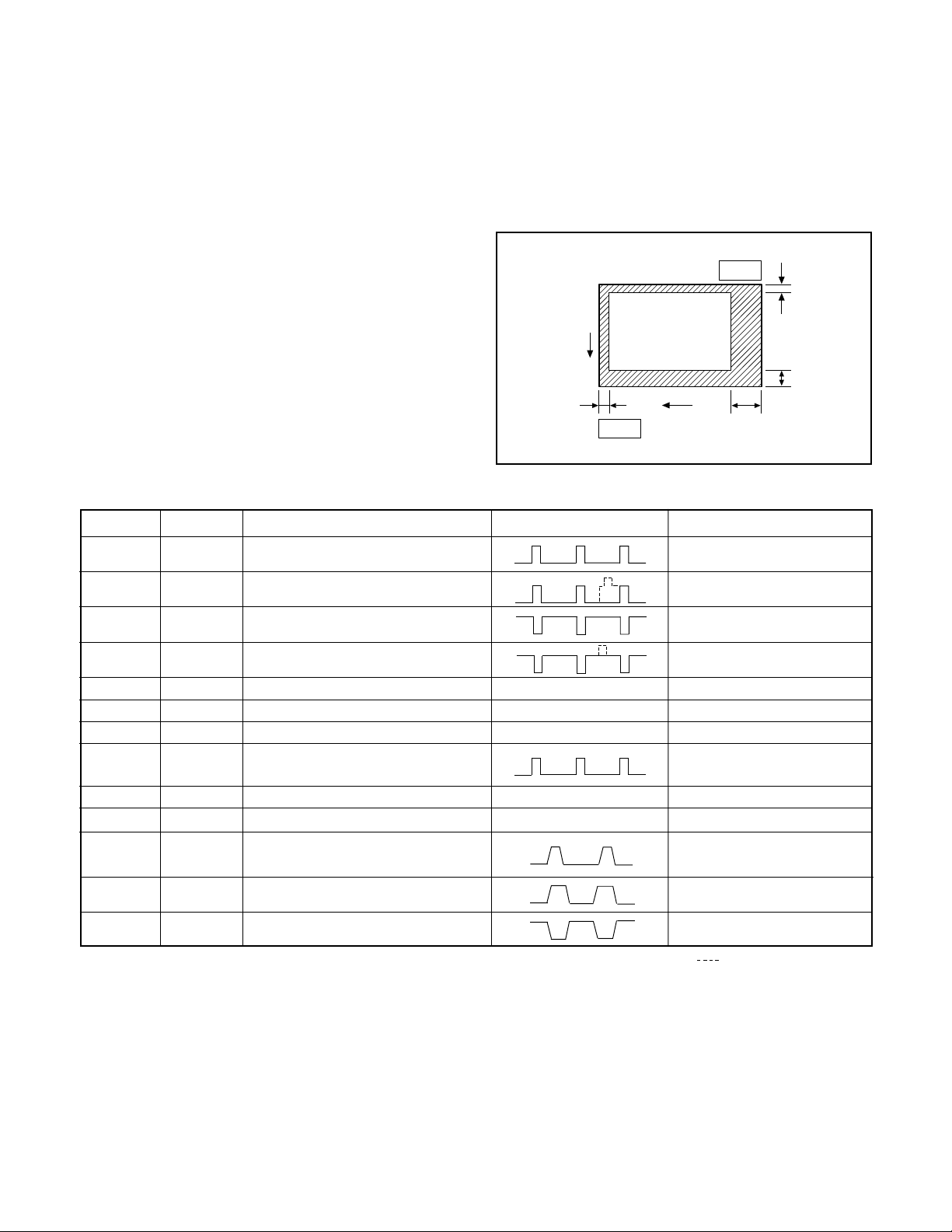
Fig. 1-1.Optical Black Location (Top View)
Pin No.
1
Symbol
2
3
4
5, 6, 7, 10
8
9
12
13
14
15
16
V φ
3
V φ1
GND
OS
OD
O
SUB
PL
φRS
φH1
φH2
Pin Description
Vertical shift register gate clock
Vertical shift register gate clock
Vertical shift register gate clock
Vertical shift register gate clock
Horizontal shift register transfer clock
Board bias
Reset transister gate clock
Horizontal shift register transfer clock
GND
Image output
Output transister drain
Protection transistor bias
Waveform
DC
Voltage
-7.5 V, 0 V
-7.5 V, 0 V, 15 V
-7.5 V, 0 V
-7.5 V, 0 V, 15 V
Amplitude 22.5 V Ex. 6 V (Bias
level is different from every CCD)
-7.5 V
0 V, 3.5 V
0 V, 3.5 V
Table 1-1. CCD Pin Description
DC
15 V
When sensor read-out
1. OUTLINE OF CIRCUIT DESCRIPTION
1-1. CA-1 CIRCUIT DESCRIPTION
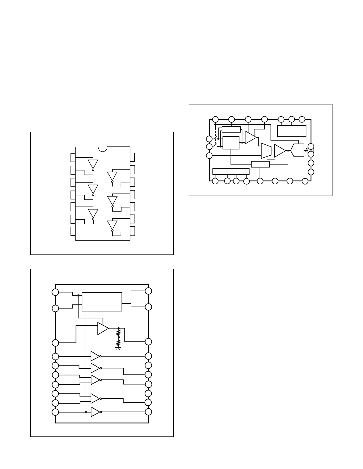
1. IC Configuration
IC903 (ICX204AK) CCD imager
IC902 (74VHC04MTC) H driver
IC904 (CXD1267AN) V driver
IC905 (AD9802) CDS/AGC, A/D converter
2. IC903 (CCD)
[Structure]
Interline type CCD image sensor
Optical size 1/3 inch format
Effective pixels 1034 (H) ×779 (V)
Pixels in total 1077 (H) ×788 (V)
Chip size 5.80 mm (H) ×4.92 mm (V)
Unit cell size 4.65 μm (H) × 4.65 μ m (H)
Optical black
Horizontal (H) direction: Front 3 pixels, Rear 40 pixels
Vertical (V) direction: Front 7 pixels, Rear 2 pixels
Dummy bit number Horizontal : 29 Vertical : 1
V φ
2B
Amplitude 3.5 V Ex. 5 V, 10 V
(Different from every CCD)
V φ2A
[Features]
Independent storage and retrieval for each pixel
Square pixel unit cell
XGA compatible
R, G, B primary color mosaic filter
Continuous variable speed electronic shutter function
11 φSUB Board clock
(Different from every CCD) Ex. 6V
−3−
1A
1
1Y
2
2A
3
2Y
4
3A
5
3Y
6
GND
7
4Y
8
4A
9
5Y
10
5A
11
6Y
12
6A
13
V
CC
14
Fig. 1-2. IC902 Block Diagram
1
18
10
9
8
7
6
5
4
3
2
14
15
16
17
20
19
11
12
13
CPP1
CPP2
DC OUT
VSHT
V
φ1
VL
Vφ2
Vφ4
VM
Vφ3
XV4
CPP3
VH
DCIN
XSHT
XV2
XV1
XSG1
XV3
XSG2
+
‑
Change Pump
Fig. 1-3. IC904 Block Diagram
3. IC902 (H Driver) and IC904 (V Driver)
An H driver (IC902) and V driver (IC904) are necessary in
order to generate the clocks (vertical transfer clock, horizon-
tal transfer clock and electronic shutter clock) which driver
the CCD.
IC902 is an inverter IC which drives the horizontal CCDs (H1
and H2). In addition the XV1-XV4 signals which are output
from Pins (166), (167), (169) and (171) of IC102 are the ver-
tical transfer clocks, and the XSG1 and XSG2 signals which
is output from Pins (168) and (170) of IC102 is superimposed
onto XV1 and XV3 at IC904 in order to generate a ternary
pulse. In addition, the XSUB signal which is output from Pin
(165) of IC102 is used as the sweep pulse for the electronic
shutter, and the RG signal which is output from Pin (159) of
IC102 is the reset gate clock.
4. IC905 (CDS, AGC Circuit and A/D converter)
The video signal which is output from the CCD is input to
Pins (26) and (27) of IC905. There are S/H blocks inside IC905
generated from the XSHP and XSHD pulses, and it is here
that CDS (correlated double sampling) is carried out.
After passing through the CDS circuit, the signal passes
through the AGC amplifier. It is A/C converted internally into
a 10-bit signal, and is then input to IC102 of the CA2 circuit
board. The gain of the AGC amplifier is controlled by the volt-
age at pin (29) which is output from IC102 of the CA2 circuit
board and smoothed by the PWM.
Fig. 1-4. IC905 Block Diagram
27
29
36
26
16
22
21
30
2319
11
12
17
PBLK
A/D
ACVDD
CMLEVEL
VRT
VTB
STBYCLPOB
ADCMODE
TIMING
GENERATOR
CLPDM PGACONT1
PGACONT2
SHP
SHD ADCCLK
PIN
DIN
ADCIN
DOUT
DRVDD
DVDD
ADVDD
2
37 20
18
47
48
43
3341
CLAMP
REFERENCE
CLAMP
CDS
PGA
MUX S/H
AD9802
10
−4−
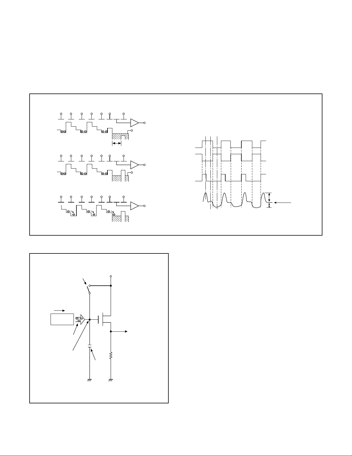
Fig. 1-5. Horizontal Transfer of CCD Imager and Extraction of Signal Voltage
Fig. 1-6. Theory of Signal Extraction Operation
H1 H2 H1 H2 H1 HOG RG
CCD OUT
PD
Floating diffusion
(1)
H1 H2 H1 H2 H1 HOG RG
CCD OUT
PD
(2)
H1 H2 H1 H2 H1 HOG RG
CCD OUT
(3)
H1
H2
RG
CCD OUT
3.5V
0V
3.5V
0V
13.5V
0V
Black level
RG pulse peak signal
Signal voltage
(1) (2) (3)
Reset gate pulse
12V Pre-charge drain bias(PD)
Direction of transfer
Voltage output
Electric
charge
H Register
Floating diffusion gate is
floated at a high impedance.
C is charged
equivalently
5. Transfer of Electric Charge by the Horizontal CCD
The transfer system for the horizontal CCD emplays a 2-phase drive method.
The electric charges sent to the final stage of the horizontal CCD are transferred to the floating diffusion, as shown in Fig. 1-5.
RG is turned on by the timing in (1), and the floating diffusion is charged to the potential of PD. The RG is turned off by the timing
in (2). In this condition, the floating diffusion is floated at high impedance. The H1 potential becomes shallow by the timing in (3),
and the electric charge now moves to the floating diffusion.
Here, the electric charges are converted into voltages at the rate of V = Q/C by the equivalent capacitance C of the floating
diffusion. RG is then turned on again by the timing in (1) when the H1 potential becomes deep.
Thus, the potential of the floating diffusion changes in proportion to the quantity of transferred electric charge, and becomes
CCD output after being received by the source follower. The equivalent circuit for the output circuit is shown in Fig. 1-6.
RG pulse leak signal

−5−
1-2. CA2 CIRCUIT DESCRIPTION
1. Circuit Description
1-1. Scannning converter (Interlace converter)
This circuit uses the function of a 64-Mbit SDRAMs to con-
vert the non-interlaced signal which is output from the CCD
into an interlaced signal for the video monitor.
1-2. Camera signal processor
This comprises circuits such as the digial clamp circuit, white
balance circuit, γcircuit, color signal generation circuit, ma-
trix circuit and horizontal aperture circuit.
1. Digital clamp circuit
The optical black section of the CCD extracts 16-pixel aver-
aged values from the subsequent data to make the black level
of the CCD output data uniform for each line. The 16-pixel
averaged value for each line is taken as the sum of the value
for the previous line multiplied by the coefficient k and the
value for the current line multiplied by the coefficient 1-k.
2. White balance circuit
This circuit controls the white balance by using the A WB judge-
ment value computed by the CPU to control the gain for each
R, G and B pixel based on the CCD data which has been
read.
3. γ circuit
This circuit performs (gamma) correction in order to maintain
a linear relat ionship b etween the light i nput to the camer a
and the light output from the picture screen.
4. Color generation circuit
This circuit converts the CCD da ta int o RGB signal s.
5. Matrix circuit
This circuit generates the Y s ignals , R-Y signals and B-Y sig-
nals from the RGB signals.
6. Horizontal aperture circuit
This circuit is used generate the aperture signal.
1-3. SDRAM controller
This circuit outputs address, RAS, CAS and AS data for con-
trolling the SDRAM. It also refr eshes the S DRA M.
1-4. PIO
The expansion parallel port can be used for functions such
as stroboscope control and LCD driver control.
1-5. SIO (Serial control)
This is the interface for the 8-bit mic roprocessor.
1-6. TG, SG block
This is the timing generation circuit which generates the clocks
(vertical transfer clock and electronic shutter clock) which drive
the CCD.
1-7. 8-bit D/A circuit (Audio)
This circuit converts the audio signals (analog signals) from
the microphone to 8-bit digital signals.
1-8. 8-bit A/D circuit (Audio)
The audio signals which were converted to digial form by the
8-bit A/D circuit are temporarily to a sound buffer and then
recorded in the SSFDC card. During playback, the 8-bit D/A
circuit converts these signals into analog audio signals.
1-9. Sound buffer
Audio memory
1-10. LCD driver
The Y/C signals which are input to the LCD driver are con-
verted to RGB signals, and the timing signal which is neces-
sary for LCD monitor display and the RGB signals are then
supplied to the LCD monitor.
1-11. LCD monitor
This is the image display device which displays the image
signals supplied from the LCD driver.
1-12. UART
This circuit is used for transmitting serial data to a PC. The
interface is RS-232C-compatible.
1-13. SSFDC control
This reads data from the SSFDC card and stores it in SDRAM,
and writes out the image data stored in SDRAM. In addition,
error correction is carried out when the data is read.
1-14. MJPEG compression
Still and continuous frame data is converted to JPEG format,
and movie images are compressed and expanded in MJPEG
format.
2. Outline of Operation
When the shutter opens, the reset signals, TEST0, TEST1
and the serial signals (“take a picture” commands) from the
8-bit microprocessor are input and record operation starts.
When the TG drives the CCD, picture data passes through
the A/D and is then input to the ASIC as 10-bit data. This data
then passes through the DCLP, AWB, shutter and γcircuit,
after which it is input to the SDRAM. The AWB, shutter, γ,
and AGC value are computed from this data, and two expo-
sures are made to obtain the optimum picture. The data which
has already been stored in the SDRAM is read by the CPU
and color generation is carried out. Each pixel is interpolated
from the surrounding data as being either R, G or B primary
color data to produce R, G and B data. At this time, correction
of the lens distortion which is a characteristic of wide-angle
lenses is carried out. Aperture correction is carried out, and
in case of still picture the data is then compressed by the
JPEG method and in case of picture it is compressed by
MJPEG method and is written to SSFDC card. When the data
is to be output to an external device, it is read JPEG picture
data from the SSFCD card and output to PC via the UART.

−6−
3. LCD Block
During EE, gamma conversion is carried out for the 10-bit
RGB data which is input from the A/D conversion block of the
CCD to the ASIC in order that the γrevised can be displayed
on the video. The YUV of 640 x 480 is then transferred to the
SVRAM.
The data which has accumulated in the SDRAM is after D/A
conversion is carried out by SDRAM control circuit inside the
ASIC , makes Y/C signal, the data is sent to the LCD panel
and displayed.
If the shutter button is pressed in this condition, the 10-bit
data which is output from the A/D conversion block of the
CCD is sent to the SDRAM (DMA transfer), and is displayed
on the LCD as a freeze-frame image.
During playback, the JPEG image data which has accumu-
lated in the SSFDC card is converted to RGB signals. In the
same way as for EE, the data is then sent to the SDRAM,
after which D/A conversion is carried out inside the ASIC,
and then the data is sent to the LCD panel and displayed.
The LCD driver is converted Y/C signals to RGB signals from
ASIC, and these RGB signals and the control signal which is
output by the LCD driver are used to drive the LCD panel.
The RGB signals are 1H transposed so that no DC compo-
nent is present in the LCD element, and the two horizontal
shift register clocks drive the horizontal shift registers inside
the LCD panel so that the 1H transposed RGB signals are
applied to the LCD panel.
Because the LCD closes more as the difference in potential
between the VCOM (common polar voltage: fixed at DC) and
the R, G and B signals becomes greater, the display becomes
darker; if the difference in potential is smaller, the element
opens and the LCD become brighter. In addition, the bright-
ness and contrast settings for the LCD can be varied by means
of the serial data from the ASIC.

−7−
1-3. PW1 POWER CIRCUIT DESCRIPTION
1. Outline
This is the main power circuit, and is comprised of the follow-
ing blocks.
Switching controller (IC501)
Digital and analog system and LCD 5.0 V system power out-
put (L5010, Q5002, D5013, C5061)
Digital 3.3 V system power supply (L5017, Q5009, D5007,
C5062)
Analog and LCD system power supply (Q5007, T5001)
Backlight power supply output (L5005, Q5008, D5014, C5005)
2. Switching Controller (IC501)
This is the basic circuit which is necessary for controlling the
power supply for a PWM-type switching regulator, and is pro-
vided with four built-in channels, only CH1 (digital 3.3 V), CH2
(5 V system), CH3 (analog and LCD system) and CH4 (back-
light system) are used. Feedback from 3.3 V (D) (CH1) ,5.0 V
(D) (CH2), +15.0 V (A), +12.4 V (L) (CH3) and 5.8 V (L) (CH4)
power supply outputs are received, and the PWM duty is var-
ied so that each one is maintained at the correct voltage set-
ting level.
2-1. Short-circuit protection circuit
If output is short-circuited for the length of time determined
by the condenser which is connected to Pin (17) of IC501, all
output is turned off. The control signal (P ON, P(A) ON and
LCD ON) are recontrolled to restore output.
3. Digital 3.3 V Power Output
3.3 V (D) is output. Feedback for the 3.3 V (D) is provided to
the switching controller (Pins (1) of IC501) so that PWM con-
trol can be carried out.
4. 5 V System Power Output
5 V (D), 5.1 V (A) and 5 V (L) are output. Feedback for the 5
V (D) is provided to the switching controller (Pin (12) of IC501)
so that PWM control can be carried out.
5. Analog and LCD System Power Output
15.0 V (A), -7.5 V (A), 12.4 V (L) and 15 V (L) are output.
Feedback for the 15.0 V (A) with view mode and 12.4 V (L)
with play mode is provided to the switching controller (Pin
(25) of IC501) so that PWM control can be carried out.
6. Backlight Power Supply output
5.8 V (L) is output. Feedback is sent to pins (36) of the switch-
ing controller (IC501) for PWM control to be carried out.

−8−
1-4. PW1 STROBE CIRCUIT DESCRIPTION
1. Charging Circuit
When UNREG power is supplied to the charge circuit and the
CHG signal becomes High (3.3 V), the charging circuit starts
operating and the main electorolytic capacitor is charged with
high-voltage direct current.
However, when the CHG signal is Low (0 V), the charging
circuit does not operate.
1-1. Power switch
When the CHG signal switches to Hi, Q5406 turns ON and
the charging circuit starts operating.
1-2. Power supply filter
L5401 and C5401 constitute the power supply filter. They
smooth out ripples in the current which accompany the switch-
ing of the oscillation transformer.
1-3. Oscillation circuit
This circuit generates an AC voltage (pulse) in order to in-
crease the UNREG power supply voltage when drops in cur-
rent occur. This circuit generates a drive pulse with a frequency
of approximately 50-100 kHz. Because self-excited light omis-
sion is used, the oscillation frequency changes according to
the drive conditions.
1-4. Oscillation transformer
The low-voltage alternating current which is generated by the
oscillation control circuit is converted to a high-voltage alter-
nating current by the oscillation transformer.
1-5. Rectifier circuit
The high-voltage alternating current which is generated at
the secondary side of T5401 is rectified to produce a high-
voltage direct current and is accumulated at electrolytic ca-
pacitor C5412 on the main circuit board.
1-6. Voltage monitoring circuit
This circuit is used to maintain the voltage accumulated at
C5412 at a constance level.
After the charging voltage is divided and converted to a lower
voltage by R5417 and R5419, it is output to the SY1 circuit
board as the monitoring voltage VMONIT. When this VMONIT
voltage reaches a specified level at the SY1 circuit board, the
CHG signal is switched to Low and charging is interrupted.
2. Light Emission Circuit
When RDY and TRIG signals are input from the ASIC expan-
sion port, the stroboscope emits light.
2-1. Emission control circuit
When the RDY signal is input to the emission control circuit,
Q5409 switches on and preparation is made to let current
flow to the light emitting element. Moreover, when a STOP
signal is input, the stroboscope stops emitting light.
2-2. Trigger circuit
When a TRIG signal is input to the trigger circuit, D5405
switches on, a high-voltage pulse of several kilovolts is gen-
erated inside the trigger circuit, and this pulse is then applied
to the light emitting part.
2-3. Light emitting element
When the high-voltage pulse form the trigger circuit is ap-
plied to the light emitting part, currnet flows to the light emit-
ting element and light is emitted.
※ Beware of electric shocks.
−9−
Pin Signal
1
3~7
8
9
10
11
13
14~19
20
21
22
31
32~69
70
71
73
74
75
76
77
78
79
80
81
82
84
86
87
88~90
83
85
91~93
CHG VOL
SCAN IN 0~4
AVREF
STBY (R) LED
STBY (G) LED
VSS
NOT USED
AVREF ON
NOT USED
CHG ON
NOT USED
VSS
NOT USED
P (A) ON
P ON
DIN CONNECT
NOT USED
AV JACK
SO
SCK
IC
XOUT
XIN
VDD
XCIN
XCOUT
RESET
BAT OFF
RXD
S. REQ
NOT USED
SCAN OUT 0~2
I/O
I
I
I
O
O
-
O
-
O
-
O
-
-
-
O
O
I
-
I
I
O
O
-
O
I
-
I
O
I
I
I
I
-
O
Outline
Strobe charge voltage input (analog input)
Key matrix input
A/D converter standard voltage input terminal
Standby LED (red) ON/OFF signal L : LED light
Standby LED (green) ON/OFF signal L : LED light
GND
Self-timer LED (red) ON/OFF signal L : LED light
-
A/D standard power ON/OFF signal L : ON
-
Flash charge ON/OFF signal H : ON
-
GND
-
DC/DC converter (analog) ON/OFF signal H : ON
DC/DC converter (digital) ON/OFF signal H : ON
DIN jack connect detection signal L : Connection
-
AV output cable connection detection signal L : Connection
Serial communication data input (←ASIC)
Serial communication data output (→ASIC)
Serial communication clock output (→ASIC)
Connect to Vss
Main clock oscillation terminal (4 MHz)
Main clock oscillation terminal
Power supply terminal
Sub clock oscillation terminal (32.768 kHz)
Sub clock oscillation terminal
Reset input
Battery OFF detection signal L : OFF
RS-232C RXD input terminal
Serial communication request signal L : Request
-
Key matrix output
1-5. SY1 CIRCUIT DESCRIPTION
1. Configuration and Functions
For the overall configuration of the SY1 circuit board, refer to the block diagram. The configuration of the SY1 circuit board
centers around a 8-bit microprocessor (IC301).
The 8-bit microprocessor handles the following functions.
1. Operation key input, 2. Mode LCD display, 3. Clock control, 4. Power ON/OFF, 5. Storobe charge control
SI
72
23~30
12
SELF LED (R)
95
96
97
98
99
100
LCD ON
ASIC TEST 0
ASIC RESET
AVSS
BATTERY
O
O
O
O
-
I
LCD monitor power ON/OFF signal H : ON
ASIC reset signal L : Reset output
ASIC reset control signal
A/D converter GND power terminal
Battery voltage input (analog input)
ASIC reset control signal
ASIC TEST 1
94
NOT USED
-
-
Table 4-1. 8-bit Microprocessor Port Specification
AVDD
-
A/D converter analog power terminal
2
NOT USED
-
-
 Loading...