


 Loading...
Samsung F8275X, F8274X, C8278X, F8278X, S3C8275X User Manual
...S3C8275X/F8275X/C8278X
/F8278X/C8274X/F8274X
8-BIT CMOS
MICROCONTROLLERS USER'S MANUAL
Revision 1.4

Important Notice
The information in this publication has been carefully checked and is believed to be entirely accurate at the time of publication. Samsung assumes no responsibility, however, for possible errors or omissions, or for any consequences resulting from the use of the information contained herein.
Samsung reserves the right to make changes in its products or product specifications with the intent to improve function or design at any time and without notice and is not required to update this documentation to reflect such changes.
This publication does not convey to a purchaser of semiconductor devices described herein any license under the patent rights of Samsung or others.
Samsung makes no warranty, representation, or guarantee regarding the suitability of its products for any particular purpose, nor does Samsung assume any liability arising out of the application or use of any product or circuit and specifically disclaims any and all liability, including without limitation any consequential or incidental damages.
"Typical" parameters can and do vary in different applications. All operating parameters, including "Typicals" must be validated for each customer application by the customer's technical experts.
Samsung products are not designed, intended, or authorized for use as components in systems intended for surgical implant into the body, for other applications intended to support or sustain life, or for any other application in which the failure of the Samsung product could create a situation where personal injury or death may occur.
Should the Buyer purchase or use a Samsung product for any such unintended or unauthorized application, the Buyer shall indemnify and hold Samsung and its officers, employees, subsidiaries, affiliates, and distributors harmless against all claims, costs, damages, expenses, and reasonable attorney fees arising out of, either directly or indirectly, any claim of personal injury or death that may be associated with such unintended or unauthorized use, even if such claim alleges that Samsung was negligent regarding the design or manufacture of said product.
S3C8275X/F8275X/C8278X/F8278X/C8274X/F8274X 8-Bit CMOS Microcontrollers User's Manual, Revision 1.4
Publication Number: 21.4-S3-C8275X/F8275X/C8278X/F8278X/C8274X/F8274X-042007
© 2007 Samsung Electronics
All rights reserved. No part of this publication may be reproduced, stored in a retrieval system, or transmitted in any form or by any means, electric or mechanical, by photocopying, recording, or otherwise, without the prior written consent of Samsung Electronics.
Samsung Electronics' microcontroller business has been awarded full ISO-14001 certification (BSI Certificate No. FM24653). All semiconductor products are designed and manufactured in accordance with the highest quality standards and objectives.
Samsung Electronics Co., Ltd.
San #24 Nongseo-Dong, Giheung-Gu
Yongin-City, Gyeonggi-Do, Korea
C.P.O. Box #37, Suwon 446-711
TEL: (82)-(31)-209-5238
FAX: (82)-(31)-209-6494
Home-Page URL: Http://www.samsungsemi.com
Printed in the Republic of Korea
NOTIFICATION OF REVISIONS
ORIGINATOR: |
Samsung Electronics, LSI Development Group, Gi-Heung, South Korea |
|
PRODUCT NAME: |
S3C8275X/F8275X/C8278X/F8278X/C8274X/F8274X 8-bit |
|
|
CMOS Microcontroller |
|
DOCUMENT NAME: |
S3C8275X/F8275X/C8278X/F8278X/C8274X/F8274X User's Manual, |
|
|
Revision1.4 |
|
DOCUMENT NUMBER: |
21.4-S3-C8275X/F8275X/C8278X/F8278X/C8274X/F8274X-042007 |
|
EFFECTIVE DATE: |
April, 2007 |
|
SUMMARY: |
As a result of additional product testing and evaluation, some specifications |
|
|
published in the S3C8275X/F8275X/C8278X/F8278X/C8274X/F8274X User's |
|
|
Manual, Revision 1, have been changed. These changes for |
|
|
S3C8275X/F8275X/C8278X/F8278X/C8274X/F8274X microcontroller, |
|
|
which are described in detail in the Revision Descriptions section below, |
|
|
are related to the followings: |
|
|
— |
Chapter 16. Embedded flash memory interface |
|
— |
Chapter 17. Electrical Data |
|
— |
Chapter 7. Clock Circuit |
|
— |
Chapter 2. Address Spaces |
DIRECTIONS: Please note the changes in your copy (copies) of the S3C8275X/F8275X/C8278X/F8278X/C8274X/F8274X User's Manual, Revision 1. Or, simply attach the Revision Descriptions of the next page to S3C8275X/F8275X/C8278X/F8278X/C8274X/F8274X User's Manual, Revision 1.
REVISION HISTORY
Revision |
Date |
0 |
February, 2005 |
|
|
1 |
April, 2005 |
1.1 |
July, 2005 |
1.2 |
August, 2005 |
|
|
1.3 |
May, 2006 |
1.4 |
April, 2007 |
|
|
Remark
Preliminary spec for internal release only. First edition. Reviewed by Finechips. Second edition. Reviewed by Finechips. Third edition. Reviewed by Finechips. Fourth edition. Reviewed by Finechips Fifth edition. Reviewed by Finechips

REVISION DESCRIPTIONS
1. Electrical Data
|
|
Table 17-12. A.C. Electrical Characteristics for Internal Flash ROM |
|
|
|
|
||||||||
(T |
A |
= − 25 °C to + 85 °C, V |
DD |
= 2.0 V to |
3.6 V) |
|
|
|
|
|
|
|
|
|
|
|
|
|
|
|
|
|
|
|
|
|
|||
|
|
Parameter |
|
|
Symbol |
Conditions |
Min |
Typ |
|
Max |
Unit |
|||
Programming time (1) |
|
|
Ftp |
− |
30 |
|
− |
|
− |
µs |
||||
Chip erasing time (2) |
|
|
Ftp1 |
|
|
|
|
|
|
|
|
ms |
||
|
|
− |
50 |
|
− |
|
− |
|||||||
|
|
|
|
|
|
|
|
|
|
|
|
|||
Sector erasing time (3) |
|
|
Ftp2 |
− |
10 |
|
− |
|
− |
ms |
||||
Data access time |
|
|
FtRS |
− |
|
− |
25 |
|
− |
ns |
||||
Number of writing/erasing |
|
|
FNwe |
|
|
|
|
|
|
|
|
Times |
||
|
|
− |
|
− |
− |
10,000(4) |
||||||||
|
|
|
|
|
|
|
|
|
|
|
|
|
|
|
NOTES:
1.The programming time is the time during which one byte (8-bit) is programmed.
2.The chip erasing time is the time during which all 16K byte block is erased.
3.The sector erasing time is the time during which all 128 byte block is erased.
4.Maximum number of writing/erasing is 10,000 times for full-flash(S3F8275) and 100 times for half-flash (S3F8278X/F8274X).
5.The chip erasing is available in Tool Program Mode only.
2. Condition of Operating Voltage
Condition of operating voltage is modified “fx = 0 − 4.2MHz” to “fx = 0.4 − 4.2MHz” at 2.0V – 3.6V and “fx = 0 − 8MHz” to “fx = 0.4 − 8MHz” at 2.5V − 3.6V in the page 17-2.
3. CHAPTHER 16. Embedded Flash Memory Interface
This chapter is modified for only S3F8275X.
4. CHAPTHER 7. Clock Circuit
The contents of OSCCON.7 should be changed “ 0 = Select normal circuit for sub oscillator” into “ 0 = Initial state” in the page 4-21 and Figure 7-10.
It is added “NOTE: The OSCCON.7 should be maintained to “1”, during the sub oscillator operation.” In the page 4-21 and Figure 7-10.
The figure 7-7 is modified partly.
Descriptions of Revision 1.4
1. Smart Option Area
The Figures are modified about smart option area. Those are “Figure 2-1. Program Memory Address Space” and “Figure 5-3. ROM Vector Address Area”.
2. CHAPTHER 17. Electrical Data
It is changed “VDD = 2.0 V to 3.6 V” into “VDD = 2.2 V to 3.6 V” in the Table 17-12.
3. DEVICE NAME
The device name is changed S3C8275/F8275/C8278/F8278/C8274/F8274 to S3C8275X/F8275X/C8278X/F8278X/C8274X/F8274X. The ‘X’ means ‘Commercial type’.
Preface
The S3C8275X/F8275X/C8278X/F8278X/C8274X/F8274X Microcontroller User's Manual is designed for application designers and programmers who are using the S3C8275X/F8275X/C8278X/F8278X/C8274X/F8274X microcontroller for application development. It is organized in two main parts:
Part I Programming Model |
Part II Hardware Descriptions |
Part I contains software-related information to familiarize you with the microcontroller's architecture, programming model, instruction set, and interrupt structure. It has six chapters:
Chapter 1 |
Product Overview |
Chapter 4 |
Control Registers |
Chapter 2 |
Address Spaces |
Chapter 5 |
Interrupt Structure |
Chapter 3 |
Addressing Modes |
Chapter 6 |
Instruction Set |
Chapter 1, "Product Overview," is a high-level introduction to S3C8275X/F8275X/C8278X/F8278X/C8274X/F8274X with general product descriptions, as well as detailed information about individual pin characteristics and pin circuit types.
Chapter 2, "Address Spaces," describes program and data memory spaces, the internal register file, and register addressing. Chapter 2 also describes working register addressing, as well as system stack and user-defined stack operations.
Chapter 3, "Addressing Modes," contains detailed descriptions of the addressing modes that are supported by the S3C8-series CPU.
Chapter 4, "Control Registers," contains overview tables for all mapped system and peripheral control register values, as well as detailed one-page descriptions in a standardized format. You can use these easy-to-read, alphabetically organized, register descriptions as a quick-reference source when writing programs.
Chapter 5, "Interrupt Structure," describes the S3C8275X/F8275X/C8278X/F8278X/C8274X/F8274X interrupt structure in detail and further prepares you for additional information presented in the individual hardware module descriptions in Part II.
Chapter 6, "Instruction Set," describes the features and conventions of the instruction set used for all S3C8-series microcontrollers. Several summary tables are presented for orientation and reference. Detailed descriptions of each instruction are presented in a standard format. Each instruction description includes one or more practical examples of how to use the instruction when writing an application program.
A basic familiarity with the information in Part I will help you to understand the hardware module descriptions in Part II. If you are not yet familiar with the S3C8-series microcontroller family and are reading this manual for the first time, we recommend that you first read Chapters 1–3 carefully. Then, briefly look over the detailed information in Chapters 4, 5, and 6. Later, you can reference the information in Part I as necessary.
Part II "hardware Descriptions," has detailed information about specific hardware components of the S3C8275X/F8275X/C8278X/F8278X/C8274X/F8274X microcontroller. Also included in Part II are electrical, mechanical, Flash MCU, and development tools data. It has 14 chapters:
Chapter 7 |
Clock Circuit |
Chapter 15 |
Battery Level Detector |
Chapter 8 |
RESET and Power-Down |
Chapter 16 |
Embedded Flash Memory Interface |
Chapter 9 |
I/O Ports |
Chapter 17 |
Electrical Data |
Chapter 10 |
Basic Timer |
Chapter 18 |
Mechanical Data |
Chapter 11 |
Timer 1 |
Chapter 19 |
S3F8275X/F8278X/F8274X |
Chapter 12 |
Watch Timer |
|
Flash MCU |
Chapter 13 |
LCD Controller/Driver |
Chapter 20 |
Development Tools |
Chapter 14 |
Serial I/O Interface |
|
|
S3C8275X/F8275X/C8278X/F8278X/C8274X/F8274X MICROCONTROLLER |
iii |
Table of Contents
Part I — Programming Model
Chapter 1 |
Product Overview |
|
S3C8-Series Microcontrollers ....................................................................................................................... |
1-1 |
|
S3C8275X/F8275X/C8278X/F8278X/C8274X/F8274X Microcontroller....................................................... |
1-1 |
|
Flash.............................................................................................................................................................. |
|
1-1 |
Features ........................................................................................................................................................ |
|
1-2 |
Block Diagram ............................................................................................................................................... |
|
1-3 |
Pin Assignment ............................................................................................................................................. |
|
1-4 |
Pin Descriptions ............................................................................................................................................ |
|
1-6 |
Pin Circuits .................................................................................................................................................... |
|
1-8 |
Chapter 2 |
Address Spaces |
|
Overview........................................................................................................................................................ |
|
2-1 |
Program Memory (ROM)............................................................................................................................... |
2-2 |
|
Smart Option......................................................................................................................................... |
|
2-3 |
Register Architecture..................................................................................................................................... |
|
2-5 |
Register Page Pointer (PP) .................................................................................................................. |
2-8 |
|
Register Set 1 ....................................................................................................................................... |
|
2-10 |
Register Set 2 ....................................................................................................................................... |
|
2-10 |
Prime Register Space........................................................................................................................... |
2-11 |
|
Working Registers ................................................................................................................................ |
2-12 |
|
Using the Register Points ..................................................................................................................... |
2-13 |
|
Register Addressing...................................................................................................................................... |
|
2-15 |
Common Working Register Area (C0H–CFH) ..................................................................................... |
2-17 |
|
4-Bit Working Register Addressing ...................................................................................................... |
2-18 |
|
8-Bit Working Register Addressing ...................................................................................................... |
2-20 |
|
System and User Stack................................................................................................................................. |
2-22 |
|
Chapter 3 |
Addressing Modes |
|
Overview........................................................................................................................................................ |
|
3-1 |
Register Addressing Mode (R)...................................................................................................................... |
3-2 |
|
Indirect Register Addressing Mode (IR)........................................................................................................ |
3-3 |
|
Indexed Addressing Mode (X)....................................................................................................................... |
3-7 |
|
Direct Address Mode (DA) ............................................................................................................................ |
3-10 |
|
Indirect Address Mode (IA) ........................................................................................................................... |
3-12 |
|
Relative Address Mode (RA)......................................................................................................................... |
3-13 |
|
Immediate Mode (IM) |
.................................................................................................................................... |
3-14 |
S3C8275X/F8275X/C8278X/F8278X/C8274X/F8274X MICROCONTROLLER |
v |
|
Table of Contents (Continued) |
|
Chapter 4 |
Control Registers |
|
Overview....................................................................................................................................................... |
|
4-1 |
Chapter 5 |
Interrupt Structure |
|
Overview....................................................................................................................................................... |
|
5-1 |
Interrupt Types..................................................................................................................................... |
|
5-2 |
S3C8275X/C8278X/C8274X Interrupt Structure ................................................................................. |
5-3 |
|
Interrupt Vector Addresses .................................................................................................................. |
5-4 |
|
Enable/Disable Interrupt Instructions (EI, DI) ...................................................................................... |
5-6 |
|
System-Level Interrupt Control Registers............................................................................................ |
5-6 |
|
Interrupt Processing Control Points ..................................................................................................... |
5-7 |
|
Peripheral Interrupt Control Registers ................................................................................................. |
5-8 |
|
System Mode Register (SYM) ............................................................................................................. |
5-9 |
|
Interrupt Mask Register (IMR) ............................................................................................................. |
5-10 |
|
Interrupt Priority Register (IPR)............................................................................................................ |
5-11 |
|
Interrupt Request Register (IRQ)......................................................................................................... |
5-13 |
|
Interrupt Pending Function Types........................................................................................................ |
5-14 |
|
Interrupt Source Polling Sequence ...................................................................................................... |
5-15 |
|
Interrupt Service Routines ................................................................................................................... |
5-15 |
|
Generating Interrupt Vector Addresses ............................................................................................... |
5-16 |
|
Nesting of Vectored Interrupts ............................................................................................................. |
5-16 |
|
Instruction Pointer (IP) ......................................................................................................................... |
5-16 |
|
Fast Interrupt Processing..................................................................................................................... |
5-16 |
|
Chapter 6 |
Instruction Set |
|
Overview....................................................................................................................................................... |
|
6-1 |
Data Types........................................................................................................................................... |
|
6-1 |
Register Addressing............................................................................................................................. |
6-1 |
|
Addressing Modes ............................................................................................................................... |
6-1 |
|
Flags Register (FLAGS)....................................................................................................................... |
6-6 |
|
Flag Descriptions ................................................................................................................................. |
6-7 |
|
Instruction Set Notation........................................................................................................................ |
6-8 |
|
Condition Codes .................................................................................................................................. |
6-12 |
|
Instruction Descriptions........................................................................................................................ |
6-13 |
|
vi |
S3C8275X/F8275X/C8278X/F8278X/C8274X/F8274X MICROCONTROLLER |
|
Table of Contents (Continued) |
|
|
Part II Hardware Descriptions |
|
Chapter 7 |
Clock Circuit |
|
Overview........................................................................................................................................................ |
|
7-1 |
System Clock Circuit ............................................................................................................................ |
7-1 |
|
Main Oscillator Circuits......................................................................................................................... |
7-2 |
|
Sub Oscillator Circuits .......................................................................................................................... |
7-2 |
|
Clock Status During Power-Down Modes ............................................................................................ |
7-3 |
|
System Clock Control Register (CLKCON) .......................................................................................... |
7-4 |
|
Clock Output Control Register (CLOCON)........................................................................................... |
7-5 |
|
Oscillator Control Register (OSCCON) ................................................................................................ |
7-6 |
|
Switching the CPU Clock...................................................................................................................... |
7-7 |
|
Chapter 8 |
RESET and Power-Down |
|
System Reset ................................................................................................................................................ |
|
8-1 |
Overview............................................................................................................................................... |
|
8-1 |
Normal Mode Reset Operation............................................................................................................. |
8-1 |
|
Hardware Reset Values........................................................................................................................ |
8-2 |
|
Power-Down Modes ...................................................................................................................................... |
|
8-5 |
Stop Mode ............................................................................................................................................ |
|
8-5 |
Idle Mode .............................................................................................................................................. |
|
8-6 |
Chapter 9 |
I/O Ports |
|
Overview........................................................................................................................................................ |
|
9-1 |
Port Data Registers .............................................................................................................................. |
9-2 |
|
port 0..................................................................................................................................................... |
|
9-3 |
port 1..................................................................................................................................................... |
|
9-7 |
port 2..................................................................................................................................................... |
|
9-11 |
port 3..................................................................................................................................................... |
|
9-13 |
Port 4 .................................................................................................................................................... |
|
9-15 |
Port 5 .................................................................................................................................................... |
|
9-17 |
Port 6 .................................................................................................................................................... |
|
9-19 |
Chapter 10 |
Basic Timer |
|
Overview........................................................................................................................................................ |
|
10-1 |
Basic Timer Control Register (BTCON) ............................................................................................... |
10-2 |
|
Basic Timer Function Description......................................................................................................... |
10-3 |
|
S3C8275X/F8275X/C8278X/F8278X/C8274X/F8274X MICROCONTROLLER |
vii |
Table of Contents (Continued)
Chapter 11 |
Timer 1 |
|
One 16-bit Timer Mode (Timer 1) ................................................................................................................. |
11-1 |
|
Overview |
.............................................................................................................................................. |
11-1 |
Function Description ............................................................................................................................ |
11-1 |
|
Two 8-bit Timers ......................................................................................................Mode (Timer A and B) |
11-4 |
|
Overview .............................................................................................................................................. |
|
11-4 |
Function Description ............................................................................................................................ |
11-4 |
|
Chapter 12 |
Watch Timer |
|
Overview....................................................................................................................................................... |
|
12-1 |
Watch Timer Control Register (WTCON) ............................................................................................ |
12-2 |
|
Watch Timer Circuit Diagram............................................................................................................... |
12-3 |
|
Chapter 13 |
LCD Controller/Driver |
|
Overview....................................................................................................................................................... |
|
13-1 |
LCD Circuit Diagram ............................................................................................................................ |
13-2 |
|
LCD RAM Address Area ...................................................................................................................... |
13-3 |
|
LCD Control Register (LCON) ............................................................................................................. |
13-4 |
|
LCD Voltage Dividing Resistor ............................................................................................................ |
13-5 |
|
Common (COM) Signals...................................................................................................................... |
13-6 |
|
Segment (SEG) Signals....................................................................................................................... |
13-6 |
|
Chapter 14 |
Serial I/O Interface |
|
Overview....................................................................................................................................................... |
|
14-1 |
Programming Procedure...................................................................................................................... |
14-1 |
|
SIO Control Registers (SIOCON) ........................................................................................................ |
14-2 |
|
SIO Pre-Scaler Register (SIOPS)........................................................................................................ |
14-3 |
|
SIO Block Diagram ....................................................................................................................................... |
|
14-3 |
Serial I/O Timing Diagram (SIO).......................................................................................................... |
14-4 |
|
Chapter 15 |
Battery Level Detector |
|
Overview....................................................................................................................................................... |
|
15-1 |
Battery Level Detector Control Register (BLDCON)............................................................................ |
15-2 |
|
viii |
S3C8275X/F8275X/C8278X/F8278X/C8274X/F8274X MICROCONTROLLER |
Table of Contents (Continued)
Chapter 16 |
Embedded Flash Memory Interface |
|
Overview........................................................................................................................................................ |
|
16-1 |
User Program Mode ...................................................................................................................................... |
|
16-2 |
Flash Memory Control Registers (User Program Mode)...................................................................... |
16-2 |
|
ISPTM (On-Board Programming) Sector ....................................................................................................... |
16-5 |
|
Sector Erase.................................................................................................................................................. |
|
16-7 |
Programming................................................................................................................................................. |
|
16-9 |
Reading ......................................................................................................................................................... |
|
16-11 |
Hard Lock Protection..................................................................................................................................... |
|
16-12 |
Chapter 17 |
Electrical Data |
|
Overview........................................................................................................................................................ |
|
17-1 |
Chapter 18 |
Mechanical Data |
|
Overview........................................................................................................................................................ |
|
18-1 |
Chapter 19 |
S3F8275X/F8278X/F8274X Flash MCU |
|
Overview........................................................................................................................................................ |
|
19-1 |
Operating Mode Characteristics........................................................................................................... |
19-5 |
|
Chapter 20 |
Development Tools |
|
Overview........................................................................................................................................................ |
|
20-1 |
SHINE................................................................................................................................................... |
|
20-1 |
SAMA Assembler.................................................................................................................................. |
20-1 |
|
SASM88................................................................................................................................................ |
|
20-1 |
HEX2ROM ............................................................................................................................................ |
|
20-1 |
Target Boards ....................................................................................................................................... |
|
20-1 |
TB8275/8/4 Target Board ..................................................................................................................... |
20-3 |
|
SMDS2+ Selection (SAM8) .................................................................................................................. |
20-6 |
|
Idle LED ................................................................................................................................................ |
|
20-6 |
Stop LED .............................................................................................................................................. |
|
20-6 |
S3C8275X/F8275X/C8278X/F8278X/C8274X/F8274X MICROCONTROLLER |
ix |
List of Figures
Figure |
Title |
Page |
Number |
|
Number |
1-1 |
Block Diagram ............................................................................................................ |
1-3 |
1-2 |
S3C8275X/F8275X/C8278X/F8278X/C8274X/F8274X Pin Assignments |
|
|
(64-QFP-1420F) ......................................................................................................... |
1-4 |
1-3 |
S3C8275X/F8275X/C8278X/F8278X/C8274X/F8274X Pin Assignments |
|
|
(64-LQFP-1010) ......................................................................................................... |
1-5 |
1-4 |
Pin Circuit Type A....................................................................................................... |
1-8 |
1-5 |
Pin Circuit Type B (nRESET) ..................................................................................... |
1-8 |
1-6 |
Pin Circuit Type E-4 (P0, P1) ..................................................................................... |
1-8 |
1-7 |
Pin Circuit Type H-4 ................................................................................................... |
1-9 |
1-8 |
Pin Circuit Type H-8 (P2.1–P2.7, P3)......................................................................... |
1-9 |
1-9 |
Pin Circuit Type H-9 (P4, P5, P6)............................................................................... |
1-10 |
1-10 |
Pin Circuit Type H-10 (P2.0)....................................................................................... |
1-11 |
2-1 |
Program Memory Address Space .............................................................................. |
2-2 |
2-2 |
Smart Option............................................................................................................... |
2-3 |
2-3 |
Internal Register File Organization (S3C8275X)........................................................ |
2-6 |
2-4 |
Internal Register File Organization (S3C8278X/C8274X).......................................... |
2-7 |
2-5 |
Register Page Pointer (PP) ........................................................................................ |
2-8 |
2-6 |
Set 1, Set 2, Prime Area Register, and LCD Data Register Map............................... |
2-11 |
2-7 |
8-Byte Working Register Areas (Slices)..................................................................... |
2-12 |
2-8 |
Contiguous 16-Byte Working Register Block ............................................................. |
2-13 |
2-9 |
Non-Contiguous 16-Byte Working Register Block ..................................................... |
2-14 |
2-10 |
16-Bit Register Pair .................................................................................................... |
2-15 |
2-11 |
Register File Addressing ............................................................................................ |
2-16 |
2-12 |
Common Working Register Area................................................................................ |
2-17 |
2-13 |
4-Bit Working Register Addressing ............................................................................ |
2-19 |
2-14 |
4-Bit Working Register Addressing Example ............................................................. |
2-19 |
2-15 |
8-Bit Working Register Addressing ............................................................................ |
2-20 |
2-16 |
8-Bit Working Register Addressing Example ............................................................. |
2-21 |
2-17 |
Stack Operations ........................................................................................................ |
2-22 |
3-1 |
Register Addressing ................................................................................................... |
3-2 |
3-2 |
Working Register Addressing..................................................................................... |
3-2 |
3-3 |
Indirect Register Addressing to Register File............................................................. |
3-3 |
3-4 |
Indirect Register Addressing to Program Memory ..................................................... |
3-4 |
3-5 |
Indirect Working Register Addressing to Register File .............................................. |
3-5 |
3-6 |
Indirect Working Register Addressing to Program or Data Memory.......................... |
3-6 |
3-7 |
Indexed Addressing to Register File .......................................................................... |
3-7 |
3-8 |
Indexed Addressing to Program or Data Memory with Short Offset .......................... |
3-8 |
3-9 |
Indexed Addressing to Program or Data Memory...................................................... |
3-9 |
3-10 |
Direct Addressing for Load Instructions ..................................................................... |
3-10 |
3-11 |
Direct Addressing for Call and Jump Instructions ...................................................... |
3-11 |
3-12 |
Indirect Addressing..................................................................................................... |
3-12 |
3-13 |
Relative Addressing.................................................................................................... |
3-13 |
3-14 |
Immediate Addressing................................................................................................ |
3-14 |
4-1 |
Register Description Format....................................................................................... |
4-4 |
S3C8275X/F8275X/C8278X/F8278X/C8274X/F8274X MICROCONTROLLER |
xi |
List of Figures
Figure |
Title |
Page |
Number |
|
Number |
5-1 |
S3C8-Series Interrupt Types ..................................................................................... |
5-2 |
5-2 |
S3C8275X/C8278X/C8274X Interrupt Structure ....................................................... |
5-3 |
5-3 |
ROM Vector Address Area ........................................................................................ |
5-4 |
5-4 |
Interrupt Function Diagram ........................................................................................ |
5-7 |
5-5 |
System Mode Register (SYM) ................................................................................... |
5-9 |
5-6 |
Interrupt Mask Register (IMR) ................................................................................... |
5-10 |
5-7 |
Interrupt Request Priority Groups .............................................................................. |
5-11 |
5-8 |
Interrupt Priority Register (IPR) ................................................................................. |
5-12 |
5-9 |
Interrupt Request Register (IRQ)............................................................................... |
5-13 |
6-1 |
System Flags Register (FLAGS) ............................................................................... |
6-6 |
7-1 |
Crystal/Ceramic Oscillator (fx) ................................................................................... |
7-2 |
7-2 |
External Oscillator (fx)................................................................................................ |
7-2 |
7-3 |
RC Oscillator (fx)........................................................................................................ |
7-2 |
7-4 |
Crystal Oscillator (fxt)................................................................................................. |
7-2 |
7-5 |
External Oscillator (fxt)............................................................................................... |
7-2 |
7-6 |
System Clock Circuit Diagram ................................................................................... |
7-3 |
7-7 |
System Clock Control Register (CLKCON) ............................................................... |
7-4 |
7-8 |
Clock Output Control Register (CLOCON) ................................................................ |
7-5 |
7-9 |
Clock Output Block Diagram...................................................................................... |
7-5 |
7-10 |
Oscillator Control Register (OSCCON) ..................................................................... |
7-6 |
7-11 |
STOP Control Register (STPCON)............................................................................ |
7-8 |
9-1 |
S3C8275X/C8278X/C8274X I/O Port Data Register Format .................................... |
9-2 |
9-2 |
Port 0 High-Byte Control Register (P0CONH)........................................................... |
9-4 |
9-3 |
Port 0 Low-Byte Control Register (P0CONL) ............................................................ |
9-4 |
9-4 |
Port 0 Pull-up Control Register (P0PUR) .................................................................. |
9-5 |
9-5 |
External Interrupt Control Register, Low Byte (EXTICONL)...................................... |
9-5 |
9-6 |
External Interrupt Pending Register (EXTIPND) ....................................................... |
9-6 |
9-7 |
Port 1 High-Byte Control Register (P1CONH)........................................................... |
9-8 |
9-8 |
Port 1 Low-Byte Control Register (P1CONL) ............................................................ |
9-8 |
9-9 |
Port 1 Pull-up Control Register (P1PUR) .................................................................. |
9-9 |
9-10 |
External Interrupt Control Register, High Byte (EXTICONH) .................................... |
9-9 |
9-11 |
External Interrupt Control Register, Low Byte (EXTICONL)...................................... |
9-10 |
9-12 |
External Interrupt Pending Register (EXTIPND) ....................................................... |
9-10 |
9-13 |
Port 2 High-byte Control Register (P2CONH) ........................................................... |
9-11 |
9-14 |
Port 2 Low-byte Control Register (P2CONL)............................................................. |
9-12 |
9-15 |
Port 2 Pull-up Control Register (P2PUR) .................................................................. |
9-12 |
9-16 |
Port 3 High Byte Control Register (P3CONH) ........................................................... |
9-13 |
9-17 |
Port 3 Low Byte Control Register (P3CONL) ............................................................ |
9-14 |
9-18 |
Port 3 Pull-up Control Register (P3PUR) .................................................................. |
9-14 |
xii |
S3C8275X/F8275X/C8278X/F8278X/C8274X/F8274X MICROCONTROLLER |
List of Figures (Continued)
Page |
Title |
Page |
Number |
|
Number |
9-19 |
Port 4 High-Byte Control Register (P4CONH) ........................................................... |
9-15 |
9-20 |
Port 4 Low-Byte Control Register (P4CONL)............................................................. |
9-16 |
9-21 |
Port 5 High-Byte Control Register (P5CONH) ........................................................... |
9-17 |
9-22 |
Port 5 Low-Byte Control Register (P5CONL)............................................................. |
9-18 |
9-23 |
Port 6 Control Register (P6CON) ............................................................................... |
9-19 |
10-1 |
Basic Timer Control Register (BTCON) ..................................................................... |
10-2 |
10-2 |
Basic Timer Block Diagram ........................................................................................ |
10-4 |
11-1 |
Timer 1/A Control Register (TACON)......................................................................... |
11-2 |
11-2 |
Timer 1 Block Diagram (One 16-bit Mode) ................................................................ |
11-3 |
11-3 |
Timer 1/A Control Register (TACON)......................................................................... |
11-5 |
11-4 |
Timer B Control Register (TBCON)............................................................................ |
11-6 |
11-5 |
Timer A Block Diagram(Two 8-bit Timers Mode) ....................................................... |
11-7 |
11-6 |
Timer B Block Diagram (Two 8-bit Timers Mode) ...................................................... |
11-8 |
12-1 |
Watch Timer Control Register (WTCON)................................................................... |
12-2 |
12-2 |
Watch Timer Circuit Diagram ..................................................................................... |
12-3 |
13-1 |
LCD Function Diagram............................................................................................... |
13-1 |
13-2 |
LCD Circuit Diagram................................................................................................... |
13-2 |
13-3 |
LCD Display Data RAM Organization ........................................................................ |
13-3 |
13-4 |
LCD Control Register (LCON).................................................................................... |
13-4 |
13-5 |
Internal Voltage Dividing Resistor Connection........................................................... |
13-5 |
13-6 |
Select/No-Select Signals in Static Display Mode ....................................................... |
13-6 |
13-7 |
Select/No-Select Signal in 1/2 Duty, 1/2 Bias Display Mode ..................................... |
13-7 |
13-8 |
Select/No-Select Signal in 1/3 Duty, 1/3 Bias Display Mode ..................................... |
13-7 |
13-9 |
LCD Signals and Wave Forms Example in 1/4 Duty, 1/3 Bias Display Mode............ |
13-8 |
14-1 |
Serial I/O Module Control Register (SIOCON)........................................................... |
14-2 |
14-2 |
SIO Prescaler Register (SIOPS) ................................................................................ |
14-3 |
14-3 |
SIO Functional Block Diagram ................................................................................... |
14-3 |
14-4 |
Serial I/O Timing in Transmit/Receive Mode (Tx at falling, SIOCON.4 = 0) .............. |
14-4 |
14-5 |
Serial I/O Timing in Transmit/Receive Mode (Tx at rising, SIOCON.4 = 1) ............... |
14-4 |
15-1 |
Block Diagram for Voltage Level Detect..................................................................... |
15-1 |
15-2 |
Battery Level Detect Circuit and Control Register...................................................... |
15-2 |
16-1 |
Flash Memory Control Register (FMCON)................................................................. |
16-2 |
16-2 |
Flash Memory User-Programming Enable Register (FMUSR) .................................. |
16-3 |
16-3 |
Flash Memory Sector Address Register, High Byte (FMSECH) ................................ |
16-4 |
16-4 |
Flash Memory Sector Address Register, Low Byte (FMSECL) ................................. |
16-4 |
16-5 |
Program Memory Address Space .............................................................................. |
16-5 |
16-6 |
Sector Configurations in User Program Mode ........................................................... |
16-7 |
S3C8275X/F8275X/C8278X/F8278X/C8274X/F8274X MICROCONTROLLER |
xiii |
List of Figures (Concluded)
Page |
Title |
Page |
Number |
|
Number |
17-1 |
Stop Mode Release Timing When Initiated by an External Interrupt |
......................... 17-5 |
17-2 |
Stop Mode Release Timing When Initiated by a RESET .......................................... |
17-6 |
17-3 |
Input Timing for External Interrupts ........................................................................... |
17-7 |
17-4 |
Input Timing for RESET ............................................................................................. |
17-8 |
17-5 |
Serial Data Transfer Timing....................................................................................... |
17-8 |
17-6 |
LVR (Low Voltage Reset) Timing .............................................................................. |
17-9 |
17-7 |
Clock Timing Measurement at XIN............................................................................. |
17-11 |
17-8 |
Clock Timing Measurement at XTIN .......................................................................... |
17-12 |
17-9 |
Operating Voltage Range .......................................................................................... |
17-13 |
18-1 |
64-Pin QFP Package Dimensions (64-QFP-1420F) ................................................. |
18-1 |
18-2 |
64-Pin LQFP Package Dimensions (64-LQFP-1010)................................................ |
18-2 |
19-1 |
S3F8275X/F8278X/F8274X Pin Assignments (64-QFP-1420F) ............................... |
19-2 |
19-2 |
S3F8275X/F8278X/F8274X Pin Assignments (64-LQFP-1010) ............................... |
19-3 |
19-3 |
Operating Voltage Range .......................................................................................... |
19-7 |
20-1 |
SMDS Product Configuration (SMDS2+)................................................................... |
20-2 |
20-2 |
TB8275/8/4 Target Board Configuration.................................................................... |
20-3 |
20-3 |
40-Pin Connectors (J101, J102) for TB8275/8/4....................................................... |
20-7 |
20-4 |
S3E8270 Cables for 64-QFP Package...................................................................... |
20-7 |
xiv |
S3C8275X/F8275X/C8278X/F8278X/C8274X/F8274X MICROCONTROLLER |
List of Tables
Table |
Title |
Page |
Number |
|
Number |
1-1 |
S3C8275X/F8275X/C8278X/F8278X/C8274X/F8274X Pin Descriptions ................. |
1-6 |
2-1 |
S3C8275X Register Type Summary.......................................................................... |
2-5 |
2-2 |
S3C8278X/C8274X Register Type Summary............................................................ |
2-5 |
4-1 |
Set 1 Registers........................................................................................................... |
4-1 |
4-2 |
Set 1, Bank 0 Registers.............................................................................................. |
4-2 |
4-3 |
Set 1, Bank 1 Registers.............................................................................................. |
4-3 |
5-1 |
Interrupt Vectors......................................................................................................... |
5-5 |
5-2 |
Interrupt Control Register Overview........................................................................... |
5-6 |
5-3 |
Interrupt Source Control and Data Registers............................................................. |
5-8 |
6-1 |
Instruction Group Summary ....................................................................................... |
6-2 |
6-2 |
Flag Notation Conventions......................................................................................... |
6-8 |
6-3 |
Instruction Set Symbols.............................................................................................. |
6-8 |
6-4 |
Instruction Notation Conventions ............................................................................... |
6-9 |
6-5 |
Opcode Quick Reference........................................................................................... |
6-10 |
6-6 |
Condition Codes......................................................................................................... |
6-12 |
8-1 |
S3C8275X/C8278X/C8274X Set 1 Register and Values After RESET..................... |
8-2 |
8-2 |
S3C8275X/C8278X/C8274X Set 1, Bank 0 Register Values After RESET............... |
8-3 |
8-3 |
S3C8275X/C8278X/C8274X Set 1, Bank 1 Register Values After RESET............... |
8-4 |
9-1 |
S3C8275X/C8278X/C8274X Port Configuration Overview ....................................... |
9-1 |
9-2 |
Port Data Register Summary ..................................................................................... |
9-2 |
13-1 |
LCD Clock Signal Frame Frequency ......................................................................... |
13-3 |
15-1 |
BLDCON Value and Detection Level ......................................................................... |
15-2 |
16-1 |
ISP Sector Size .......................................................................................................... |
16-6 |
16-2 |
Reset Vector Address ................................................................................................ |
16-6 |
S3C8275X/F8275X/C8278X/F8278X/C8274X/F8274X MICROCONTROLLER |
xv |
List of Tables (Continued)
Table |
Title |
Page |
Number |
|
Number |
17-1 |
Absolute Maximum Ratings........................................................................................ |
17-2 |
17-2 |
D.C. Electrical Characteristics.................................................................................... |
17-2 |
17-3 |
Data Retention Supply Voltage in Stop Mode ............................................................ |
17-5 |
17-4 |
Input/Output Capacitance........................................................................................... |
17-6 |
17-5 |
A.C. Electrical Characteristics .................................................................................... |
17-7 |
17-6 |
Battery Level Detector Electrical Characteristics ....................................................... |
17-9 |
17-7 |
LVR (Low Voltage Reset) Electrical Characteristics .................................................. |
17-9 |
17-8 |
Main Oscillation Characteristics ................................................................................. |
17-10 |
17-9 |
Sub Oscillation Characteristics................................................................................... |
17-10 |
17-10 |
Main Oscillation Stabilization Time............................................................................. |
17-11 |
17-11 |
Sub Oscillation Stabilization Time .............................................................................. |
17-12 |
17-12 |
A.C. Electrical Characteristics for Internal Flash ROM .............................................. |
17-13 |
19-1 |
Descriptions of Pins Used to Read/Write the Flash ROM.......................................... |
19-4 |
19-2 |
Comparison of S3F8275X/F8278X/F8274X and |
|
|
S3C8275X/C8278X/C8274X Features....................................................................... |
19-4 |
19-3 |
Operating Mode Selection Criteria ............................................................................. |
19-5 |
19-4 |
D.C. Electrical Characteristics.................................................................................... |
19-6 |
20-1 |
Power Selection Settings for TB8275/8/4................................................................... |
20-4 |
20-2 |
Main-clock Selection Settings for TB8275/8/4............................................................ |
20-4 |
20-3 |
Select Smart Option Source Setting for TB8275/8/4.................................................. |
20-5 |
20-4 |
Smart Option Switch Settings for TB8275/8/4............................................................ |
20-5 |
20-5 |
Device Selection Settings for TB8275/8/4.................................................................. |
20-6 |
20-6 |
The SMDS2+ Tool Selection Setting.......................................................................... |
20-6 |
xvi |
S3C8275X/F8275X/C8278X/F8278X/C8274X/F8274X MICROCONTROLLER |
List of Programming Tips
Description |
|
Page |
Chapter 2: |
Address Spaces |
Number |
|
||
Using the Page Pointer for RAM Clear (Page 0, Page 1) ........................................................................ |
2-9 |
|
Setting the Register Pointers.................................................................................................................... |
2-13 |
|
Using the RPs to Calculate the Sum of a Series of Registers ................................................................. |
2-14 |
|
Addressing the Common Working Register Area..................................................................................... |
2-18 |
|
Standard Stack Operations Using PUSH and POP ................................................................................. |
2-23 |
|
Chapter 5: |
Interrupt Structure |
|
How to clear an interrupt pending bit........................................................................................................ |
5-15 |
|
Chapter 7: |
Clock Circuit |
|
Switching the CPU Clock.......................................................................................................................... |
7-7 |
|
Chapter 16: |
Embedded Flash Memory Interface |
|
Sector Erase ............................................................................................................................................. |
16-8 |
|
Program |
.................................................................................................................................................... |
16-10 |
Reading..................................................................................................................................................... |
|
16-11 |
Hard Lock ................................................................................................................................Protection |
16-12 |
|
S3C8275X/F8275X/C8278X/F8278X/C8274X/F8274X MICROCONTROLLER |
xvii |
List of Register Descriptions
Register |
Full Register Name |
Page |
Identifier |
|
Number |
BLDCON |
Battery Level Detector Control Register .................................................................... |
4-5 |
BTCON |
Basic Timer Control Register ..................................................................................... |
4-6 |
CLKCON |
System Clock Control Register .................................................................................. |
4-7 |
CLOCON |
Clock Output Control Register ................................................................................... |
4-8 |
EXTICONH |
External Interrupt Control Register (High Byte) ......................................................... |
4-9 |
EXTICONL |
External Interrupt Control Register (Low Byte) .......................................................... |
4-10 |
EXITPND |
External Interrupt Pending Register ........................................................................... |
4-11 |
FLAGS |
System Flags Register ............................................................................................... |
4-12 |
FMCON |
Flash Memory Control Register ................................................................................. |
4-13 |
FMSECH |
Flash Memory Sector Address Register (High Byte) ................................................. |
4-14 |
FMSECL |
Flash Memory Sector Address Register (Low Byte).................................................. |
4-14 |
FMUSR |
Flash Memory User Programming Enable Register .................................................. |
4-15 |
IMR |
Interrupt Mask Register.............................................................................................. |
4-16 |
IPH |
Instruction Pointer (High Byte) ................................................................................... |
4-17 |
IPL |
Instruction Pointer (Low Byte) .................................................................................... |
4-17 |
IPR |
Interrupt Priority Register ........................................................................................... |
4-18 |
IRQ |
Interrupt Request Register ......................................................................................... |
4-19 |
LCON |
LCD Control Register ................................................................................................. |
4-20 |
OSCCON |
Oscillator Control Register ......................................................................................... |
4-21 |
P0CONH |
Port 0 Control Register (High Byte)............................................................................ |
4-22 |
P0CONL |
Port 0 Control Register (Low Byte) ............................................................................ |
4-23 |
P0PUR |
Port 0 Pull-Up Control Register.................................................................................. |
4-24 |
P1CONH |
Port 1 Control Register (High Byte)............................................................................ |
4-25 |
P1CONL |
Port 1 Control Register (Low Byte) ............................................................................ |
4-26 |
P1PUR |
Port 1 Pull-up Control Register .................................................................................. |
4-27 |
P2CONH |
Port 2 Control Register (High Byte)............................................................................ |
4-28 |
P2CONL |
Port 2 Control Register (Low Byte) ............................................................................ |
4-29 |
P2PUR |
Port 2 Pull-up Control Register .................................................................................. |
4-30 |
P3CONH |
Port 3 Control Register (High Byte)............................................................................ |
4-31 |
P3CONL |
Port 3 Control Register (Low Byte) ............................................................................ |
4-32 |
P3PUR |
Port 3 Pull-up Control Register .................................................................................. |
4-33 |
P4CONH |
Port 4 Control Register (High Byte)............................................................................ |
4-34 |
P4CONL |
Port 4 Control Register (Low Byte) ............................................................................ |
4-35 |
P5CONH |
Port 5 Control Register (High Byte)............................................................................ |
4-36 |
P5CONL |
Port 5 Control Register (Low Byte) ............................................................................ |
4-37 |
P6CON |
Port 6 Control Register............................................................................................... |
4-38 |
PP |
Register Page Pointer ................................................................................................ |
4-39 |
RP0 |
Register Pointer 0....................................................................................................... |
4-40 |
RP1 |
Register Pointer 1....................................................................................................... |
4-40 |
SIOCON |
SIO Control Register .................................................................................................. |
4-41 |
SPH |
Stack Pointer (High Byte)........................................................................................... |
4-42 |
SPL |
Stack Pointer (Low Byte)............................................................................................ |
4-42 |
STPCON |
Stop Control Register................................................................................................. |
4-43 |
SYM |
System Mode Register............................................................................................... |
4-44 |
TACON |
Timer 1/A Control Register......................................................................................... |
4-45 |
TBCON |
Timer B Control Register............................................................................................ |
4-46 |
WTCON |
Watch Timer Control Register.................................................................................... |
4-47 |
S3C8275X/F8275X/C8278X/F8278X/C8274X/F8274X MICROCONTROLLER |
xix |
List of Instruction Descriptions
Instruction |
Full Register Name |
Page |
Mnemonic |
|
Number |
ADC |
Add with Carry............................................................................................................ |
6-14 |
ADD |
Add ............................................................................................................................. |
6-15 |
AND |
Logical AND ............................................................................................................... |
6-16 |
BAND |
Bit AND....................................................................................................................... |
6-17 |
BCP |
Bit Compare ............................................................................................................... |
6-18 |
BITC |
Bit Complement.......................................................................................................... |
6-19 |
BITR |
Bit Reset..................................................................................................................... |
6-20 |
BITS |
Bit Set ......................................................................................................................... |
6-21 |
BOR |
Bit OR ......................................................................................................................... |
6-22 |
BTJRF |
Bit Test, Jump Relative on False ............................................................................... |
6-23 |
BTJRT |
Bit Test, Jump Relative on True................................................................................. |
6-24 |
BXOR |
Bit XOR....................................................................................................................... |
6-25 |
CALL |
Call Procedure............................................................................................................ |
6-26 |
CCF |
Complement Carry Flag ............................................................................................. |
6-27 |
CLR |
Clear ........................................................................................................................... |
6-28 |
COM |
Complement ............................................................................................................... |
6-29 |
CP |
Compare..................................................................................................................... |
6-30 |
CPIJE |
Compare, Increment, and Jump on Equal ................................................................. |
6-31 |
CPIJNE |
Compare, Increment, and Jump on Non-Equal ......................................................... |
6-32 |
DA |
Decimal Adjust ........................................................................................................... |
6-33 |
DEC |
Decrement.................................................................................................................. |
6-35 |
DECW |
Decrement Word ........................................................................................................ |
6-36 |
DI |
Disable Interrupts ....................................................................................................... |
6-37 |
DIV |
Divide (Unsigned)....................................................................................................... |
6-38 |
DJNZ |
Decrement and Jump if Non-Zero.............................................................................. |
6-39 |
EI |
Enable Interrupts ........................................................................................................ |
6-40 |
ENTER |
Enter ........................................................................................................................... |
6-41 |
EXIT |
Exit.............................................................................................................................. |
6-42 |
IDLE |
Idle Operation............................................................................................................. |
6-43 |
INC |
Increment ................................................................................................................... |
6-44 |
INCW |
Increment Word.......................................................................................................... |
6-45 |
IRET |
Interrupt Return .......................................................................................................... |
6-46 |
JP |
Jump........................................................................................................................... |
6-47 |
JR |
Jump Relative............................................................................................................. |
6-48 |
LD |
Load............................................................................................................................ |
6-49 |
LDB |
Load Bit ...................................................................................................................... |
6-51 |
S3C8275X/F8275X/C8278X/F8278X/C8274X/F8274X MICROCONTROLLER |
xxi |
List of Instruction Descriptions (Continued)
Instruction |
Full Register Name |
Page |
Mnemonic |
|
Number |
LDC/LDE |
Load Memory.............................................................................................................. |
6-52 |
LDCD/LDED |
Load Memory and Decrement.................................................................................... |
6-54 |
LDCI/LDEI |
Load Memory and Increment...................................................................................... |
6-55 |
LDCPD/LDEPD |
Load Memory with Pre-Decrement............................................................................. |
6-56 |
LDCPI/LDEPI |
Load Memory with Pre-Increment .............................................................................. |
6-57 |
LDW |
Load Word .................................................................................................................. |
6-58 |
MULT |
Multiply (Unsigned)..................................................................................................... |
6-59 |
NEXT |
Next............................................................................................................................. |
6-60 |
NOP |
No Operation .............................................................................................................. |
6-61 |
OR |
Logical OR .................................................................................................................. |
6-62 |
POP |
Pop from Stack ........................................................................................................... |
6-63 |
POPUD |
Pop User Stack (Decrementing)................................................................................. |
6-64 |
POPUI |
Pop User Stack (Incrementing) .................................................................................. |
6-65 |
PUSH |
Push to Stack.............................................................................................................. |
6-66 |
PUSHUD |
Push User Stack (Decrementing)............................................................................... |
6-67 |
PUSHUI |
Push User Stack (Incrementing) ................................................................................ |
6-68 |
RCF |
Reset Carry Flag......................................................................................................... |
6-69 |
RET |
Return ......................................................................................................................... |
6-70 |
RL |
Rotate Left .................................................................................................................. |
6-71 |
RLC |
Rotate Left through Carry ........................................................................................... |
6-72 |
RR |
Rotate Right................................................................................................................ |
6-73 |
RRC |
Rotate Right through Carry......................................................................................... |
6-74 |
SB0 |
Select Bank 0.............................................................................................................. |
6-75 |
SB1 |
Select Bank 1.............................................................................................................. |
6-76 |
SBC |
Subtract with Carry ..................................................................................................... |
6-77 |
SCF |
Set Carry Flag............................................................................................................. |
6-78 |
SRA |
Shift Right Arithmetic .................................................................................................. |
6-79 |
SRP/SRP0/SRP1 |
Set Register Pointer.................................................................................................... |
6-80 |
STOP |
Stop Operation............................................................................................................ |
6-81 |
SUB |
Subtract ...................................................................................................................... |
6-82 |
SWAP |
Swap Nibbles.............................................................................................................. |
6-83 |
TCM |
Test Complement under Mask ................................................................................... |
6-84 |
TM |
Test under Mask......................................................................................................... |
6-85 |
WFI |
Wait for Interrupt ......................................................................................................... |
6-86 |
XOR |
Logical Exclusive OR.................................................................................................. |
6-87 |
xxii |
S3C8275X/F8275X/C8278X/F8278X/C8274X/F8274X MICROCONTROLLER |

S3C8275X/F8275X/C8278X/F8278X/C8274X/F8274X |
PRODUCT OVERVIEW |
|
|
1 PRODUCT OVERVIEW
S3C8-SERIES MICROCONTROLLERS
Samsung's S3C8 series of 8-bit single-chip CMOS microcontrollers offers a fast and efficient CPU, a wide range of integrated peripherals, and various mask-programmable ROM sizes. Among the major CPU features are:
•Efficient register-oriented architecture
•Selectable CPU clock sources
•Idle and Stop power-down mode release by interrupt or reset
•Built-in basic timer with watchdog function
A sophisticated interrupt structure recognizes up to eight interrupt levels. Each level can have one or more interrupt sources and vectors. Fast interrupt processing (within a minimum of four CPU clocks) can be assigned to specific interrupt levels.
S3C8275X/F8275X/C8278X/F8278X/C8274X/F8274X MICROCONTROLLER
The S3C8275X/F8275X/C8278X/F8278X/C8274X/F8274X single-chip CMOS microcontrollers are fabricated using the highly advanced CMOS process, based on Samsung's latest CPU architecture.
The S3C8275X/C8278X/C8274X is a microcontroller with a 16/8/4K-byte mask-programmable ROM embedded.
The S3F8275X/F8278X/F8274X is a microcontroller with a 16/8/4K-byte flash ROM embedded.
Using a proven modular design approach, Samsung engineers have successfully developed the S3C8275X/F8275X/C8278X/F8278X/C8274X/F8274X by integrating the following peripheral modules with the powerful SAM8 core:
•Seven programmable I/O ports, including six 8-bit ports and one 4-bit port, for a total of 52 pins.
•Eight bit-programmable pins for external interrupts.
•One 8-bit basic timer for oscillation stabilization and watchdog function (system reset).
•Two 8-bit timer/counter with selectable operating modes.
•Watch timer for real time
FLASH
The S3F8275X/F8278X/F8274X are FLASH version of the S3C8275X/C8278X/C8274X microcontroller. The S3F8275X/F8278X/F8274X microcontroller has an on-chip FLASH ROM instead of a masked ROM. The S3F8275X/F8278X/F8274X is comparable to the S3C8275X/C8278X/C8274X, both in function and in pin configuration. The S3F8275X only is a full flash. The full flash means that data can be written into the program ROM by an instruction.
1-1

PRODUCT OVERVIEW |
S3C8275X/F8275X/C8278X/F8278X/C8274X/F8274X |
|
|
FEATURES
CPU
•SAM88RC CPU core
Memory
•Program Memory(ROM)
-16K×8 bits program memory(S3C8275X/F8275X)
-8K×8 bits program memory(S3C8278X/F8278X)
-4K×8 bits program memory(S3C8274X/F8274X)
-Internal flash memory(Program memory)
√Sector size: 128 Bytes
√10 Years data retention
√Fast programming time:
+Chip erase: 50ms
+Sector erase: 10ms
+Byte program: 30us
√User programmable by ‘LDC’ instruction
√Endurance: 10,000 erase/program cycles
√Sector(128-bytes) erase available
√Byte programmable
√External serial programming support
√Expandable OBPTM(On board program) sector
•Data Memory (RAM)
-Including LCD display data memory
-544 × 8 bits data memory(S3C8275X/F8275X)
-288 × 8 bits data memory(S3C8278X/F8278X)
-288 × 8 bits data memory(S3C8274X/F8274X)
Instruction Set
•78 instructions
•Idle and Stop instructions added for power-down modes
52 I/O Pins
•I/O: 16 pins
•I/O: 36 pins (Sharing with LCD signal outputs)
Interrupts
•8 interrupt levels and 12 interrupt sources
•Fast interrupt processing feature
8-Bit Basic Timer
•Watchdog timer function
•4 kinds of clock source
Two 8-Bit Timer/Counters
•Programmable interval timer
•External event counter function
•Configurable as one 16-bit timer/counters
Watch Timer
•Interval time: 3.91mS, 0.25S, 0.5S, and 1S at 32.768 kHz
•0.5/1/2/4 kHz Selectable buzzer output
LCD Controller/Driver
•32 segments and 4 common terminals
•Static, 1/2 duty, 1/3 duty, and 1/4 duty selectable
•Internal resistor circuit for LCD bias
8-bit Serial I/O Interface
•8-bit transmit/receive mode
•8-bit receive mode
•LSB-first or MSB-first transmission selectable
•Internal or External clock source
Battery Level Detector
•3-criteria voltage selectable (2.2V, 2.4V, 2.8V)
•En/Disable by software for current consumption source
Low Voltage Reset (LVR)
•Criteria voltage: 2.2V
•En/Disable by smart option (ROM address: 3FH)
Two Power-Down Modes
•Idle: only CPU clock stops
•Stop: selected system clock and CPU clock stop
Oscillation Sources
•Crystal, ceramic, or RC for main clock
•Main clock frequency: 0.4 MHz − 8 MHz
•32.768 kHz crystal for sub clock
Instruction Execution Times
•500nS at 8 MHz fx(minimum)
Operating Voltage Range
•2.0 V to 3.6 V at 0.4 − 4.2 MHz
•2.5 V to 3.6 V at 0.4 − 8.0 MHz
Operating Temperature Range
•−25 °C to +85 °C
Package Type
•64-QFP-1420F, 64-LQFP-1010
Smart Option
•Low Voltage Reset(LVR) level and enable/disable are at your hardwired option (ROM address 3FH)
•ISP related option selectable (ROM address 3EH)
1-2

S3C8275X/F8275X/C8278X/F8278X/C8274X/F8274X |
PRODUCT OVERVIEW |
|
|
BLOCK DIAGRAM
|
|
|
|
XIN |
XOUT |
|
Watchdog |
|
TAOUT/P0.4 |
8-Bit Timer/ |
|
nRESET |
VREG |
Timer |
|
||
16-Bit |
XTIN |
XTOUT |
|
|||||
T1CLK/P0.3 |
Basic Timer |
|
||||||
Counter A |
|
|
|
|
|
|||
TBOUT/P0.5 |
8-Bit Timer/ |
Timer/ |
|
|
|
|
|
|
Counter B |
Counter 1 |
|
|
|
|
Low Voltage |
|
|
|
|
|
|
|
|
|||
|
P0.0/INT0 |
|
|
|
|
|
Reset |
|
|
|
|
|
|
|
Clock Out |
|
|
|
P0.1/INT1 |
|
|
|
|
|
CLKOUT/P0.6 |
|
|
|
|
|
|
|
Block |
||
|
P0.2/INT2 |
|
Port I/O and Interrupt Control |
|||||
|
|
|
||||||
P0.3/T1CLK |
I/O Port 0 |
|
|
|
|
Battery Level |
VBLDREF/ |
|
P0.4/TAOUT |
|
|
|
|
||||
|
|
|
|
Detector |
P2.0/SEG31 |
|||
P0.5/TBOUT |
|
|
|
|
|
|||
|
|
|
|
|
|
|
||
P0.6/CLKOUT |
|
|
|
|
|
Watch Timer |
BUZ/P0.7 |
|
|
P0.7/BUZ |
|
|
|
|
|
|
|
|
P1.0/SCK |
|
|
|
|
|
|
COM0-COM3/P6.0-P6.3 |
|
|
|
SAM88RC CPU |
|
|
SEG0-SEG7/P5.7-P5.0 |
||
|
P1.1/SO |
|
|
|
|
|||
|
|
|
|
|
|
|
SEG8-SEG15/P4.7-P4.0 |
|
|
P1.2/SI |
|
|
|
|
|
LCD |
|
|
P1.3/INT3 |
|
|
|
|
|
SEG16-SEG23/P3.7-P3.0 |
|
|
P1.4/INT4 |
I/O Port 1 |
|
|
|
|
Driver |
|
|
P1.5/INT5 |
|
|
|
|
|
|
SEG24-SEG30/P2.7-P2.1 |
|
P1.6/INT6 |
|
|
|
|
|
|
SEG31/P2.0/VBLDREF |
|
P1.7/INT7 |
|
|
|
|
|
|
|
|
|
544/288 Byte |
16/8/4-Kbyte |
|
VLC0-VLC2 |
|||
|
|
|
|
|||||
P2.0/SEG31/VBLDREF |
|
Register File |
ROM |
|
|
P1.0/SCK |
||
I/O Port 2 |
|
|
|
|
SIO |
|||
P2.1-P2.7/SEG30-SEG24 |
|
|
|
|
P1.1/SO |
|||
|
|
|
|
|
|
P1.2/SI |
||
P3.0-P3.7/SEG23-SEG16 |
I/O Port 3 |
|
|
|
|
I/O Port 6 |
P6.0-P6.3/ |
|
|
|
|
|
COM0-COM3 |
||||
|
|
|
|
|
|
|
|
|
|
|
|
|
|
|
|
I/O Port 5 |
P5.0-P5.7/ |
P4.0-P4.7/SEG15-SEG8 |
I/O Port 4 |
|
|
|
|
SEG7-SEG0 |
||
|
|
|
|
|
||||
|
|
|
|
|
|
|||
Figure 1-1. Block Diagram
1-3
PRODUCT OVERVIEW |
S3C8275X/F8275X/C8278X/F8278X/C8274X/F8274X |
|
|
PIN ASSIGNMENT
|
|
SEG1/P5.6 |
SEG2/P5.5 SEG3/P5.4 SEG4/P5.3 SEG5/P5.2 SEG6/P5.1 SEG7/P5.0 SEG8/P4.7 SEG9/P4.6 SEG10/P4.5 SEG11/P4.4 SEG12/P4.3 SEG13/P4.2 |
|
|
|
||||||||||||||||||||||||||
|
|
|
|
|
|
|||||||||||||||||||||||||||
|
|
|
|
|
|
|
|
|
|
|
|
|
|
|
|
|
|
|
|
|
|
|
|
|
|
|
|
|
|
|
|
|
|
|
64 63 62 61 60 59 58 57 56 55 54 53 52 |
|
|
|
|||||||||||||||||||||||||||
SEG0/P5.7 |
|
1 |
|
|
|
|
|
|
|
|
|
|
|
|
|
|
|
|
|
|
|
|
|
|
|
|
|
|
|
51 |
|
SEG14/P4.1 |
|
|
|
|
|
|
|
|
|
|
|
|
|
|
|
|
|
|
|
|
|
|
|
|
|
|
|
|
|
||||
|
|
|
|
|
|
|
|
|
|
|
|
|
|
|
|
|
|
|
|
|
|
|
|
|
|
|
|
|
||||
COM0/P6.0 |
|
2 |
|
|
|
|
|
|
|
|
|
|
|
|
|
|
|
|
|
|
|
|
|
|
|
|
|
|
|
50 |
|
SEG15/P4.0 |
|
|
|
|
|
|
|
|
|
|
|
|
|
|
|
|
|
|
|
|
|
|
|
|
|
|
|
|
|
||||
|
|
|
|
|
|
|
|
|
|
|
|
|
|
|
|
|
|
|
|
|
|
|
|
|
|
|
|
|
||||
COM1/P6.1 |
|
3 |
|
|
|
|
|
|
|
|
|
|
|
|
|
|
|
|
|
|
|
|
|
|
|
|
|
|
|
49 |
|
SEG16/P3.7 |
|
|
|
|
|
|
|
|
|
|
|
|
|
|
|
|
|
|
|
|
|
|
|
|
|
|
|
|
|
||||
|
|
|
|
|
|
|
|
|
|
|
|
|
|
|
|
|
|
|
|
|
|
|
|
|
|
|
|
|
||||
COM2/P6.2 |
|
4 |
|
|
|
|
|
|
|
|
|
|
|
|
|
|
|
|
|
|
|
|
|
|
|
|
|
|
|
48 |
|
SEG17/P3.6 |
|
|
|
|
|
|
|
|
|
|
|
|
|
|
|
|
|
|
|
|
|
|
|
|
|
|
|
|
|
||||
|
|
|
|
|
|
|
|
|
|
|
|
|
|
|
|
|
|
|
|
|
|
|
|
|
|
|
|
|
||||
COM3/P6.3 |
|
5 |
|
|
|
|
|
|
|
|
|
|
|
|
|
|
|
|
|
|
|
|
|
|
|
|
|
|
|
47 |
|
SEG18/P3.5 |
|
|
|
|
|
|
|
|
|
|
|
|
|
|
|
|
|
|
|
|
|
|
|
|
|
|
|
|
|
||||
|
|
|
|
|
|
|
|
|
|
|
|
|
|
|
|
|
|
|
|
|
|
|
|
|
|
|
|
|
||||
VLC0 |
|
6 |
|
|
S3C8275X/F8275X |
46 |
|
SEG19/P3.4 |
||||||||||||||||||||||||
|
|
|
|
|||||||||||||||||||||||||||||
|
|
|
|
|||||||||||||||||||||||||||||
VLC1 |
|
7 |
|
|
45 |
|
SEG20/P3.3 |
|||||||||||||||||||||||||
|
|
|
|
|||||||||||||||||||||||||||||
|
|
|
|
|||||||||||||||||||||||||||||
VLC2 |
|
8 |
|
|
S3C8278X/F8278X |
44 |
|
SEG21/P3.2 |
||||||||||||||||||||||||
|
|
|
|
|||||||||||||||||||||||||||||
|
|
|
|
|||||||||||||||||||||||||||||
VDD |
|
9 |
|
|
43 |
|
SEG22/P3.1 |
|||||||||||||||||||||||||
|
|
|
|
|||||||||||||||||||||||||||||
VSS |
|
10 |
|
|
S3C8274X/F8274X |
42 |
|
SEG23/P3.0 |
||||||||||||||||||||||||
|
|
|
|
|||||||||||||||||||||||||||||
|
|
|
|
|||||||||||||||||||||||||||||
XOUT |
|
11 |
|
|
|
|
|
|
|
|
|
|
|
|
|
|
|
|
|
|
|
|
|
|
|
|
|
|
|
41 |
|
SEG24/P2.7 |
|
|
|
|
|
|
|
|
|
|
|
|
|
|
|
|
|
|
|
|
|
|
|
|
|
|
|
|
|
||||
|
|
|
|
|
|
|
|
|
|
|
|
|
|
|
|
|
|
|
|
|
|
|
|
|
|
|
|
|
||||
XIN |
|
12 |
|
|
|
|
|
|
(64-QFP-1420F) |
40 |
|
SEG25/P2.6 |
||||||||||||||||||||
|
|
|
|
|
|
|
|
|||||||||||||||||||||||||
|
|
|
|
|
|
|
|
|||||||||||||||||||||||||
TEST |
|
13 |
|
|
|
|
|
|
39 |
|
SEG26/P2.5 |
|||||||||||||||||||||
|
|
|
|
|
|
|
|
|||||||||||||||||||||||||
|
|
|
|
|
|
|
|
|||||||||||||||||||||||||
XTIN |
|
14 |
|
|
|
|
|
|
|
|
|
|
|
|
|
|
|
|
|
|
|
|
|
|
|
|
|
|
|
38 |
|
SEG27/P2.4 |
|
|
|
|
|
|
|
|
|
|
|
|
|
|
|
|
|
|
|
|
|
|
|
|
|
|
|
|
|
||||
|
|
|
|
|
|
|
|
|
|
|
|
|
|
|
|
|
|
|
|
|
|
|
|
|
|
|
|
|
||||
XTOUT |
|
15 |
|
|
|
|
|
|
|
|
|
|
|
|
|
|
|
|
|
|
|
|
|
|
|
|
|
|
|
37 |
|
SEG28/P2.3 |
|
|
|
|
|
|
|
|
|
|
|
|
|
|
|
|
|
|
|
|
|
|
|
|
|
|
|
|
|
||||
|
|
|
|
|
|
|
|
|
|
|
|
|
|
|
|
|
|
|
|
|
|
|
|
|
|
|
|
|
||||
nRESET |
|
16 |
|
|
|
|
|
|
|
|
|
|
|
|
|
|
|
|
|
|
|
|
|
|
|
|
|
|
|
36 |
|
SEG29/P2.2 |
|
|
|
|
|
|
|
|
|
|
|
|
|
|
|
|
|
|
|
|
|
|
|
|
|
|
|
|
|
||||
|
|
|
|
|
|
|
|
|
|
|
|
|
|
|
|
|
|
|
|
|
|
|
|
|
|
|
|
|
||||
VREG |
|
17 |
|
|
|
|
|
|
|
|
|
|
|
|
|
|
|
|
|
|
|
|
|
|
|
|
|
|
|
35 |
|
SEG30/P2.1 |
|
|
|
|
|
|
|
|
|
|
|
|
|
|
|
|
|
|
|
|
|
|
|
|
|
|
|
|
|
||||
|
|
|
|
|
|
|
|
|
|
|
|
|
|
|
|
|
|
|
|
|
|
|
|
|
|
|
|
|
||||
P0.0/INT0 |
|
18 |
|
|
|
|
|
|
|
|
|
|
|
|
|
|
|
|
|
|
|
|
|
|
|
|
|
|
|
34 |
|
SEG31/P2.0/VBLDREF |
|
|
|
|
|
|
|
|
|
|
|
|
|
|
|
|
|
|
|
|
|
|
|
|
|
|
|
|
|
||||
|
|
|
|
|
|
|
|
|
|
|
|
|
|
|
|
|
|
|
|
|
|
|
|
|
|
|
|
|
||||
P0.1/INT1 |
|
19 |
|
|
|
|
|
|
|
|
|
|
|
|
|
|
|
|
|
|
|
|
|
|
|
|
|
|
|
33 |
|
P1.7/INT7 |
|
|
|
|
|
|
|
|
|
|
|
|
|
|
|
|
|
|
|
|
|
|
|
|
|
|
|
|
|
||||
|
|
|
|
|
|
|
|
|
|
|
|
|
|
|
|
|
|
|
|
|
|
|
|
|
|
|
|
|
||||
|
|
20 21 22 23 24 25 26 27 28 29 30 31 32 |
|
|
|
|||||||||||||||||||||||||||
|
|
|
|
|
|
|
|
|
|
|
|
|
|
|
|
|
|
|
|
|
|
|
|
|
|
|
|
|
|
|
|
|
|
|
|
|
|
|
|
|
|
|
|
|
|
|
|
|
|
|
|
|
|
|
|
|
|
|
|
|
|
|
|
|
|
|
|
P0.2/INT2 |
P0.3/T1CLK P0.4/TAOUT P0.5/TBOUT P0.6/CLKOUT P0.7/BUZ P1.0/SCK P1.1/SO P1.2/SI P1.3/INT3 P1.4/INT4 P1.5/INT5 P1.6/INT6 |
|
|
|
||||||||||||||||||||||||||
Figure 1-2. S3C8275X/F8275X/C8278X/F8278X/C8274X/F8274X Pin Assignments (64-QFP-1420F)
1-4
S3C8275X/F8275X/C8278X/F8278X/C8274X/F8274X |
PRODUCT OVERVIEW |
|
|
|
|
SEG1/P5.6 |
SEG2/P5.5 |
SEG3/P5.4 SEG4/P5.3 SEG5/P5.2 SEG6/P5.1 SEG7/P5.0 SEG8/P4.7 SEG9/P4.6 SEG10/P4.5 SEG11/P4.4 SEG12/P4.3 SEG13/P4.2 SEG14/P4.1 |
SEG15/P4.0 |
SEG16/P3.7 |
|
|
||||||||||||||||||||||||||||||||
|
|
|
|
|
||||||||||||||||||||||||||||||||||||
|
|
|
|
|
|
|
|
|
|
|
|
|
|
|
|
|
|
|
|
|
|
|
|
|
|
|
|
|
|
|
|
|
|
|
|
|
|
|
|
|
|
|
64 63 62 61 60 59 58 57 56 55 54 53 52 51 50 49 |
|
|
||||||||||||||||||||||||||||||||||||
SEG0/P5.7 |
|
1 |
|
|
|
|
|
|
|
|
|
|
|
|
|
|
|
|
|
|
|
|
|
|
|
|
|
|
|
|
|
|
|
|
|
48 |
|
SEG17/P3.6 |
||
|
|
|
|
|
|
|
|
|
|
|
|
|
|
|
|
|
|
|
|
|
|
|
|
|
|
|
|
|
|
|
|
|
|
|
||||||
|
|
|
|
|
|
|
|
|
|
|
|
|
|
|
|
|
|
|
|
|
|
|
|
|
|
|
|
|
|
|
|
|
|
|
||||||
COM0/P6.0 |
|
2 |
|
|
|
|
|
|
|
|
|
|
|
|
|
|
|
|
|
|
|
|
|
|
|
|
|
|
|
|
|
|
|
|
|
47 |
|
SEG18/P3.5 |
||
|
|
|
|
|
|
|
|
|
|
|
|
|
|
|
|
|
|
|
|
|
|
|
|
|
|
|
|
|
|
|
|
|
|
|
||||||
|
|
|
|
|
|
|
|
|
|
|
|
|
|
|
|
|
|
|
|
|
|
|
|
|
|
|
|
|
|
|
|
|
|
|
||||||
COM1/P6.1 |
|
3 |
|
|
|
|
|
|
|
|
|
|
|
|
|
|
|
|
|
|
|
|
|
|
|
|
|
|
|
|
|
|
|
|
|
46 |
|
SEG19/P3.4 |
||
|
|
|
|
|
|
|
|
|
|
|
|
|
|
|
|
|
|
|
|
|
|
|
|
|
|
|
|
|
|
|
|
|
|
|
||||||
|
|
|
|
|
|
|
|
|
|
|
|
|
|
|
|
|
|
|
|
|
|
|
|
|
|
|
|
|
|
|
|
|
|
|
||||||
COM2/P6.2 |
|
4 |
|
|
|
|
|
|
|
|
|
|
|
|
|
|
|
|
|
|
|
|
|
|
|
|
|
|
|
|
|
|
|
|
|
45 |
|
SEG20/P3.3 |
||
|
|
|
|
|
|
|
|
|
|
|
|
|
|
|
|
|
|
|
|
|
|
|
|
|
|
|
|
|
|
|
|
|
|
|
||||||
|
|
|
|
|
|
|
|
|
|
|
|
|
|
|
|
|
|
|
|
|
|
|
|
|
|
|
|
|
|
|
|
|
|
|
||||||
COM3/P6.3 |
|
5 |
|
|
|
|
|
|
S3C8275X/F8275X |
|
|
|
44 |
|
SEG21/P3.2 |
|||||||||||||||||||||||||
|
|
|
|
|
|
|
|
|
|
|
||||||||||||||||||||||||||||||
|
|
|
|
|
|
|
|
|
|
|
||||||||||||||||||||||||||||||
VLC0 |
|
6 |
|
|
|
|
|
|
|
|
|
43 |
|
SEG22/P3.1 |
||||||||||||||||||||||||||
|
|
|
|
|
|
|
|
|
|
|
||||||||||||||||||||||||||||||
VLC1 |
|
7 |
|
|
|
|
|
|
S3C8278X/F8278X |
|
|
|
42 |
|
SEG23/P3.0 |
|||||||||||||||||||||||||
|
|
|
|
|
|
|
|
|
|
|
||||||||||||||||||||||||||||||
|
|
|
|
|
|
|
|
|
|
|
||||||||||||||||||||||||||||||
VLC2 |
|
8 |
|
|
|
|
|
|
S3C8274X/F8274X |
|
|
|
41 |
|
SEG24/P2.7 |
|||||||||||||||||||||||||
|
|
|
|
|
|
|
|
|
|
|
||||||||||||||||||||||||||||||
|
|
|
|
|
|
|
|
|
|
|
||||||||||||||||||||||||||||||
VDD |
|
9 |
|
|
|
|
|
|
|
|
|
40 |
|
SEG25/P2.6 |
||||||||||||||||||||||||||
|
|
|
|
|
|
|
|
|
|
|
||||||||||||||||||||||||||||||
|
|
|
|
|
|
|
|
|
|
|
||||||||||||||||||||||||||||||
VSS |
|
10 |
|
|
|
|
|
|
|
|
|
|
|
|
|
|
|
|
|
|
|
|
|
|
|
|
|
|
|
|
|
|
|
|
|
39 |
|
SEG26/P2.5 |
||
|
|
|
|
|
|
|
|
|
|
|
|
|
|
|
|
|
|
|
|
|
|
|
|
|
|
|
|
|
|
|
|
|
|
|
||||||
|
|
|
|
|
|
|
|
|
|
|
|
|
|
|
|
|
|
|
|
|
|
|
|
|
|
|
|
|
|
|
|
|
|
|
||||||
XOUT |
|
11 |
|
|
|
|
|
|
|
|
|
|
(64-LQFP-1010) |
|
|
|
38 |
|
SEG27/P2.4 |
|||||||||||||||||||||
|
|
|
|
|
|
|
|
|
|
|
|
|
|
|
||||||||||||||||||||||||||
|
|
|
|
|
|
|
|
|
|
|
|
|
|
|
||||||||||||||||||||||||||
XIN |
|
12 |
|
|
|
|
|
|
|
|
|
|
|
|
|
37 |
|
SEG28/P2.3 |
||||||||||||||||||||||
|
|
|
|
|
|
|
|
|
|
|
|
|
|
|
||||||||||||||||||||||||||
|
|
|
|
|
|
|
|
|
|
|
|
|
|
|
|
|
|
|
|
|
|
|
|
|
|
|
|
|
|
|
|
|
|
|
||||||
TEST |
|
13 |
|
|
|
|
|
|
|
|
|
|
|
|
|
|
|
|
|
|
|
|
|
|
|
|
|
|
|
|
|
|
|
|
|
36 |
|
SEG29/P2.2 |
||
|
|
|
|
|
|
|
|
|
|
|
|
|
|
|
|
|
|
|
|
|
|
|
|
|
|
|
|
|
|
|
|
|
|
|
||||||
|
|
|
|
|
|
|
|
|
|
|
|
|
|
|
|
|
|
|
|
|
|
|
|
|
|
|
|
|
|
|
|
|
|
|
||||||
XTIN |
|
14 |
|
|
|
|
|
|
|
|
|
|
|
|
|
|
|
|
|
|
|
|
|
|
|
|
|
|
|
|
|
|
|
|
|
35 |
|
SEG30/P2.1 |
||
|
|
|
|
|
|
|
|
|
|
|
|
|
|
|
|
|
|
|
|
|
|
|
|
|
|
|
|
|
|
|
|
|
|
|
||||||
|
|
|
|
|
|
|
|
|
|
|
|
|
|
|
|
|
|
|
|
|
|
|
|
|
|
|
|
|
|
|
|
|
|
|
||||||
XTOUT |
|
15 |
|
|
|
|
|
|
|
|
|
|
|
|
|
|
|
|
|
|
|
|
|
|
|
|
|
|
|
|
|
|
|
|
|
34 |
|
SEG31/P2.0/VBLDREF |
||
|
|
|
|
|
|
|
|
|
|
|
|
|
|
|
|
|
|
|
|
|
|
|
|
|
|
|
|
|
|
|
|
|
|
|
||||||
|
|
|
|
|
|
|
|
|
|
|
|
|
|
|
|
|
|
|
|
|
|
|
|
|
|
|
|
|
|
|
|
|
|
|
||||||
nRESET |
|
16 |
|
|
|
|
|
|
|
|
|
|
|
|
|
|
|
|
|
|
|
|
|
|
|
|
|
|
|
|
|
|
|
|
|
33 |
|
P1.7/INT7 |
||
|
|
|
|
|
|
|
|
|
|
|
|
|
|
|
|
|
|
|
|
|
|
|
|
|
|
|
|
|
|
|
|
|
|
|
||||||
|
|
|
|
|
|
|
|
|
|
|
|
|
|
|
|
|
|
|
|
|
|
|
|
|
|
|
|
|
|
|
|
|
|
|
||||||
|
|
17 18 19 20 21 22 23 24 25 26 27 28 29 30 31 32 |
|
|
||||||||||||||||||||||||||||||||||||
|
|
|
|
|
|
|
|
|
|
|
|
|
|
|
|
|
|
|
|
|
|
|
|
|
|
|
|
|
|
|
|
|
|
|
|
|
|
|
|
|
|
|
|
|
|
|
|
|
|
|
|
|
|
|
|
|
|
|
|
|
|
|
|
|
|
|
|
|
|
|
|
|
|
|
|
|
|
|
|
|
|
|
|
VREG |
P0.0/INT0 |
P0.1/INT1 P0.2/INT2 P0.3/T1CLK P0.4/TAOUT P0.5/TBOUT P0.6/CLKOUT P0.7/BUZ P1.0/SCK P1.1/SO P1.2/SI P1.3/INT3 P1.4/INT4 |
P1.5/INT5 |
P1.6/INT6 |
|
|
||||||||||||||||||||||||||||||||
Figure 1-3. S3C8275X/F8275X/C8278X/F8278X/C8274X/F8274X Pin Assignments (64-LQFP-1010)
1-5

PRODUCT OVERVIEW |
S3C8275X/F8275X/C8278X/F8278X/C8274X/F8274X |
|
|
PIN DESCRIPTIONS
Table 1-1. S3C8275X/F8275X/C8278X/F8278X/C8274X/F8274X Pin Descriptions
Pin |
Pin |
Pin |
Circuit |
Pin |
Shared |
Names |
Type |
Description |
Type |
No. |
Functions |
P0.0−P0.2 |
I/O |
I/O port with bit-programmable pins; |
E-4 |
18−20 |
INT0−INT2 |
P0.3 |
|
Schmitt trigger input or push-pull, open-drain |
|
21 |
T1CLK |
P0.4 |
|
output and software assignable pull-ups; |
|
22 |
TAOUT |
P0.5 |
|
P0.0−P0.2 are alternately used for external |
|
23 |
TBOUT |
P0.6 |
|
interrupt input(noise filters, interrupt enable |
|
24 |
CLKOUT |
P0.7 |
|
and pending control). |
|
25 |
BUZ |
P1.0 |
I/O |
I/O port with bit-programmable pins; |
E-4 |
26 |
SCK |
P1.1 |
|
Schmitt trigger input or push-pull, open-drain |
|
27 |
SO |
P1.2 |
|
output and software assignable pull-ups; |
|
28 |
SI |
P1.3−P1.7 |
|
P1.3−P1.7 are alternately used for external |
|
29−33 |
INT3−INT7 |
|
|
interrupt input(noise filters, interrupt enable |
|
|
|
|
|
and pending control). |
|
|
|
P2.0 |
I/O |
I/O port with bit-programmable pins; |
H-10 |
34 |
SEG31/VBLDREF |
P2.1−P2.7 |
|
Input or push-pull, open-drain output and |
H-8 |
35−41 |
SEG30−SEG24 |
|
|
software assignable pull-ups. |
|
|
|
P3.0−P3.7 |
I/O |
I/O port with bit-programmable pins; |
H-8 |
42−49 |
SEG23−SEG16 |
|
|
Input or push-pull, open-drain output and |
|
|
|
|
|
software assignable pull-ups. |
|
|
|
P4.0−P4.7 |
I/O |
I/O port with bit-programmable pins; |
H-9 |
50−57 |
SEG15−SEG8 |
P5.0−P5.7 |
|
Input or push-pull output and software |
|
58−64, 1 |
SEG7−SEG0 |
P6.0−P6.3 |
|
assignable pull-ups. |
|
2−5 |
COM0−COM3 |
1-6

S3C8275X/F8275X/C8278X/F8278X/C8274X/F8274X PRODUCT OVERVIEW
Table 1-1. S3C8275X/F8275X/C8278X/F8278X/C8274X/F8274X Pin Descriptions (Continued)
Pin |
Pin |
Pin |
Circuit |
Pin |
Shared |
Names |
Type |
Description |
Type |
No. |
Functions |
VLC0−VLC2 |
− |
LCD power supply pins. |
− |
6−8 |
− |
INT0−INT2 |
I/O |
External interrupts input pins. |
E-4 |
18−20 |
P0.0−P0.2 |
INT3−INT7 |
|
|
|
29−33 |
P1.3−P1.7 |
T1CLK |
I/O |
Timer 1/A external clock input. |
E-4 |
21 |
P0.3 |
TAOUT |
I/O |
Timer 1/A clock output. |
E-4 |
22 |
P0.4 |
|
|
|
|
|
|
TBOUT |
I/O |
Timer B clock output. |
E-4 |
23 |
P0.5 |
CLKOUT |
I/O |
System clock output. |
E-4 |
24 |
P0.6 |
BUZ |
I/O |
Output pin for buzzer signal. |
E-4 |
25 |
P0.7 |
|
|
|
|
|
|
SCK, SO, SI |
I/O |
Serial clock, data output, and data input. |
E-4 |
26,27,28 |
P1.0, P1.1, P1.2 |
COM0–COM3 |
I/O |
LCD common signal outputs. |
H-9 |
2−5 |
P6.0−P6.3 |
|
|
|
|
|
|
SEG0–SEG15 |
I/O |
LCD segment signal outputs. |
H-9 |
1,64− 50 |
P5.7−P4.0 |
SEG16–SEG30 |
|
|
H-8 |
49−35 |
P3.7−P2.1 |
SEG31 |
|
|
H-10 |
34 |
P2.0/VBLDREF |
VBLDREF |
I/O |
Battery level detector reference voltage |
H-10 |
34 |
P2.0/SEG31 |
VREG |
O |
Regulator voltage output for sub clock |
− |
17 |
− |
|
|
(needed 0.1uF) |
|
|
|
nRESET |
I |
System reset pin |
B |
16 |
− |
|
|
|
|
|
|
XTIN, XTOUT |
− |
Sub oscillator pins |
− |
14, 15 |
− |
XIN, XOUT |
− |
Main oscillator pins. |
− |
12, 11 |
− |
TEST |
I |
Test input: it must be connected to VSS |
− |
13 |
− |
VDD, VSS |
− |
Power input pins |
− |
9, 10 |
− |
1-7
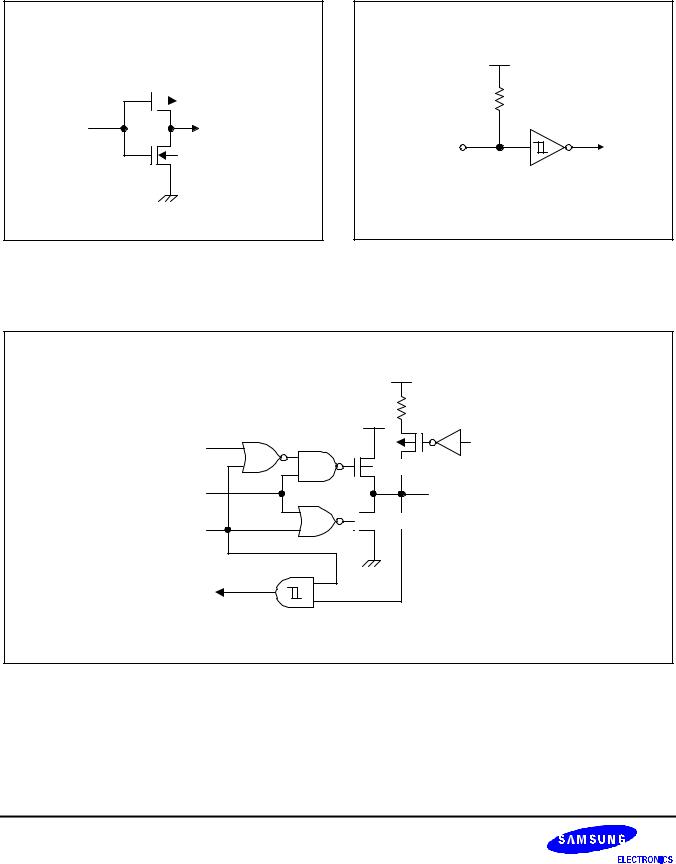
PRODUCT OVERVIEW |
S3C8275X/F8275X/C8278X/F8278X/C8274X/F8274X |
|
|
PIN CIRCUITS
VDD |
|
VDD |
|||
|
|
|
|
|
|
|
|
|
|
P-Channel |
Pull-Up |
|
|
|
|
||
|
|
|
|
Resistor |
|
|
|
|
|
||
|
|
|
|
|
|
In 
In
N-Channel
Schmitt Trigger
Figure 1-4. Pin Circuit Type A |
Figure 1-5. Pin Circuit Type B (nRESET) |
VDD
Pull-up
VDD Resistor
Open
Drain
Data |
Output |
Disable |
Resistor
Enable
 P-CH
P-CH
 I/O
I/O

 N-CH
N-CH
Schmitt Trigger
Figure 1-6. Pin Circuit Type E-4 (P0, P1)
1-8
Loading...