


601CF USER'S MANUAL
M/B For Socket 370 Pentium III Processor
NO. G03-601CFR4A
Release date: November 2001
Trademark:
*Pentium is registered trademark and MMX is a trademark of Intel Corporation, the other names and brands are the property of their respective owners
*Specifications and Information contained in this documentation are furnished for information use only, and are subject to change at any time without notice, and should not be construed as a commitment by manufacturer.

TABLE OF CONTENT
USER’S NOTICE.............................................................................. |
ii |
||
MANUAL REVISION INFORMATION ............................................. |
1 |
||
THERMAL SOLUTIONS.................................................................... |
1 |
||
CHAPTER 1 INTRODUCTION OF 601CF MOTHERBOARD |
|
||
1-1 FEATURE OF MOTHERBOARD............................................................... |
2 |
||
1-2 |
SPECIFICATION .......................................................................................... |
3 |
|
1-3 |
PERFORMANCE LIST ................................................................................ |
4 |
|
1-4 LAYOUT DIAGRAM & JUMPER SETTING ........................................... |
5 |
||
CHAPTER 2 HARDWARE INSTALLATION |
|
||
2-1 HARDWARE INSTALLATION STEPS..................................................... |
7 |
||
2-2 CHECKING MOTHERBAORD'S JUMPER SETTING .......................... |
7 |
||
2-3 |
INSTALL CPU ............................................................................................... |
8 |
|
|
2-3-1 ABOUT PENTIUM & CELERON™ 370-PIN CPU.................... |
8 |
|
|
2-3-2 SETTING CPU BUS CLOCK & MEMORY CLOCK JUMPER . 9 |
||
|
2-3-3 |
INSTALL CPU.................................................................................... |
9 |
|
2-3-4 |
OVERCLOCK RUNNING ........................................................................... |
10 |
2-4 |
INSTALL MEMORY .................................................................................... |
11 |
|
2-5 |
EXPANSION CARD ...................................................................................... |
12 |
|
|
2-5-1 PROCEDURE FOR EXPANSION CARD INSTALLATION .................. |
12 |
|
|
2-5-2 ASSIGNING IRQ FOR EXPANSION CARD............................................ |
12 |
|
|
2-5-3 INTERRUPT REQUEST TABLE FOR THIS MOTHERBOARD.......... |
13 |
|
2-6 |
CONNECTORS, HEADERS ........................................................................ |
13 |
|
|
2-6-1 CONNECTORS ............................................................................................. |
13 |
|
|
2-6-2 HEADERS ...................................................................................................... |
16 |
|
2-7 STARTING UP YOUR COMPUTER.......................................................... |
19 |
||
CHAPTER 3 INTRODUCING BIOS |
|
||
3-1 |
ENTERING SETUP....................................................................................... |
20 |
|
3-2 |
GETTING HELP............................................................................................ |
21 |
|
3-3 THE MAIN MENU ........................................................................................ |
21 |
||
3-4 STANDARD CMOS FEATURES................................................................. |
23 |
||
3-5 ADVANCED BIOS FEATURES .................................................................. |
23 |
||
3-6 ADVANCED CHIPSET FEATURES .......................................................... |
24 |
||
|
3-6-1 ADVANCED DRAM CONTROL..................................................... |
25 |
|
3-7 |
INTEGRATED PERIPHERALS.................................................................. |
26 |
|
|
3-7-1 |
ONCHIP IDE FUNCTION........................................................................... |
27 |
|
3-7-2 |
ONCHIP DEVICE FUNCTION................................................................... |
27 |
|
3-7-3 ONCHIP SUPERIO FUNCTION ................................................................ |
28 |
|
3-8 POWER MANAGEMENT SETUP.............................................................. |
28 |
||
|
3-8-1 |
POWER MANAGEMENT ........................................................................... |
29 |
|
3-8-2 |
WAKE UP EVENTS ..................................................................................... |
29 |
i

|
3-8-2.1 IRQS ACTIVITY MONITORING ........................................................... |
30 |
3-9 |
PNP/PCI CONFIGURATION SETUP........................................................ |
30 |
3-10 |
PC HEALTH STATUS................................................................................. |
31 |
3-11 |
MISCELLANEOUS CONTROL ................................................................ |
32 |
3-12 |
LOAD STANDARD/OPTIMIZED DEFAULTS ....................................... |
32 |
3-13 |
SET SUPERVISOR/USER PASSWORD ................................................... |
33 |
CHAPTER 4 DRIVER & FREE PROGRAM INSTALLATION
MAGIC INSTALL SUPPORTS WINDOWS 95/98/98SE/NT4.0/2000 ............. |
34 |
||
4-1 |
IDE INSTALL VIA IDE/AGPVXD/IRQ ROUTING/INF DRIVER .................... |
35 |
|
4-2 |
VGA INSTALL VIA 8601 VGA DRIVER ........................................................ |
37 |
|
4-3 |
SOUND |
INSTALL ALC AUDIO CODEC DRIVER FOR VIA ................ |
37 |
4-4 |
PC-HEALTH INSTALL VIA HARDWARE MONITOR DRIVER ................... |
39 |
|
|
4-4-1 HOW TO USE VIA HARDWARE MONITRO APPLICATION |
|
|
|
SOFTWARE .................................................................................................. |
39 |
|
4-5 |
MAGIC BIOS INSTALL BIOS LIVE UPDATE UTILITY................................ |
40 |
|
4-6 |
PC-CILLIN INSTALL PC-CILLIN 2000 ANTI-VIRUS PROGRAM ............ |
41 |
|
4-7 HOW TO DISABLE ON-BOARD SOUND................................................. |
43 |
||
4-8 HOW TO UPDATE BIOS ............................................................................. |
43 |
||
USER’S NOTICE
COPYRIGHT OF THIS MANUAL BELONGS TO THE MANUFACTURER. NO PART OF THIS MANUAL, INCLUDING THE PRODUCTS AND SOFTWARE DESCRIBED IN IT MAY BE REPRODUCED, TRANSMITTED OR TRANSLATED INTO ANY LANGUAGE IN ANY FORM OR BY ANY MEANS WITHOUT WRITTEN PERMISSION OF THE MANUFACTURER.
THIS MANUAL CONTAINS ALL INFORMATION REQUIRED TO USE 601CF MOTHERBOARD AND WE DO ASSURE THIS MANUAL MEETS USER’S REQUIREMENT BUT WILL CHANGE, CORRECT ANY TIME WITHOUT NOTICE. MANUFACTURER PROVIDES THIS MANUAL “AS IS” WITHOUT WARRANTY OF ANY KIND, AND WILL NOT BE LIABLE FOR ANY INDIRECT, SPECIAL, INCIDENTIAL OR CONSEQUENTIAL DAMAGES (INCLUDING DAMANGES FOR LOSS OF PROFIT, LOSS OF BUSINESS, LOSS OF USE OF DATA, INTERRUPTION OF BUSINESS AND THE LIKE).
PRODUCTS AND CORPORATE NAMES APPEARING IN THIS MANUAL MAY OR MAY NOT BE REGISTERED TRADEMARKS OR COPYRIGHTS OF THEIR RESPECTIVE COMPANIES, AND THEY ARE USED ONLY FOR IDENTIFICATION OR EXPLANATION AND TO THE OWNER’S BENEFIT, WITHOUT INTENT TO INFRINGE.
ii

Manual Revision Information
Reversion |
Revision History |
Date |
4.0 |
Fourth Edition |
November 2001 |
Item Checklist
5601CF Motherboard
5Cable for IDE/Floppy
5CD for motherboard utilities
5601CF User’s Manual
Intel Processor Family
Thermal Solutions
As processor technology pushes to faster speeds and higher performance, thermal management becomes increasingly crucial when building computer systems. Maintaining the proper thermal environment is key to reliable, long-term system operation. The overall goal in providing the proper thermal environment is keeping the processor below its specified maximum case temperature. Heatsinks induce improved processor heat dissipation through increased surface area and concentrated airflow from attached fans. In addition, interface materials allow effective transfers of heat from the processor to the heatsink. For optimum heat transfer, Intel recommends the use of thermal grease and mounting clips to attach the heatsink to the processor.
When selecting a thermal solution for your system, please refer to the website below for collection of heatsinks evaluated and recommended by Intel for use with Intel processors.
Vendor list for heatsink and fan of Pentium® !!! processor, please visit http://developer.intel.com/design/Pentiumiii/components/index.htm
Vendor list for heatsink and fan of Intel®Celeron™ processor, please visit http://developer.intel.com/design/celeron/components/index.htm
Chapter 1
1

Introduction of 601CF Motherboard
1-1 Feature of motherboard
The 601CF motherboard is design for use Intel’s new generation Pentium processors, which utilize the Socket 370 design and the memory size expandable to 1GB (using 256Mb technology). This motherboard integrated VGA, Audio, and PC Health Function with Micro ATX form factor to support total solution for today’s computer market.
This motherboard using VIA Apollo PLE133 VT8601A and VT82C686B chipset, whose 133MHz front side bus delivers a clear upgrade path to the future generation of 133MHz processors and PC-100/PC-133 SDRAM. The 601CF motherboard offers ULTRA DMA 66/100 (ATA 100) to provide speedier HDD throughout that boosts overall system performance.
The 601CF also has an integrated AC’97 2.1 CODEC on board which is fully compatible with Sound Blaster Pro that gives you the best sound quality and compatibility. VIA VT8601A chipset also includes integrated 3D Graphic Acceleration to provide a lower cost video display solution.
With USB control as well as capability of expanding to 4 USB connectors support four USB devices, the 601CF meet future USB demand. Moreover, it has built-in hardware monitor function to monitor and protect your computer.
This motherboard provides high performance & meets future specification demand. It is really wise choice for your computer.
1-2 Specification
2

Spec |
|
Description |
Design |
|
Micro ATX form factor 4 layers PCB size: 24.4 x 19.0 cm |
Chipset |
|
VIA Apollo PLE133 VT8601A and VT82C686B Chipset |
Clock Generator |
|
Winbond W83194BR-39B |
|
|
Support 66/100/133MHz system Bus Clock (CPU Bus Clock) |
|
|
Support 100/133 MHz system memory clock |
|
|
Support 33MHz PCI Bus clock |
CPU Socket |
|
Support Pentium III 500 1GHz processor |
|
|
Support Celeron 300 900MHz processor |
|
Support 66, 100 and 133MHz CPU Bus clock |
|
|
Reserves support for future Intel Pentium III processors |
|
|
Support Cyrix III series processors |
|
Memory Socket |
|
168-pin DIMM socket x2 |
|
|
PC-100/PC-133 SDRAM |
|
|
Expandable to 1GB |
|
Support 3.3V SDRAM DIMM |
|
Expansion Slot |
|
32-bit PCI slot x3 |
& Headers |
|
AMR slot x1 |
|
|
ISA slot x1 |
Integrate VGA |
|
64-bit Signal Cycle 2D/3D Graphic Engine |
|
Support 2 to 8 Mbytes of Frame Buffer |
|
Integrate IDE |
|
2 channel of Bus Master IDE port supporting ULTRA DMA |
|
|
33/66/100 mode devices |
Audio |
|
AC’97 Digital Audio controller integrated |
|
AC’97 Audio CODEC on board |
|
|
Audio driver and utility included |
|
BIOS |
|
Award 2Mb Flash ROM |
Multi I/O |
|
PS/2 keyboard and PS/2 mouse connectors |
|
Floppy disk drive connector x1 |
|
|
|
Parallel port x1 |
|
|
Serial port x2 |
|
USB connector x2, USB header x2 |
|
|
Audio connector (Line-in, Line-out/MIC & Game Port) |
|
|
|
|
1-3 Performance List
3

The following performance data list is the testing result of some popular benchmark testing programs. These data are just referred by users, and there is no responsibility for different testing data values gotten by users (the different Hardware & Software configuration will result in different benchmark testing results.)
CPU: |
Intel PIII 866MHz/Celeron 667MHz FC-PGA package |
DRAM: |
128M SDRAM x2 (Hyundai GM72V66841ET75) |
VGA Expansion Card: Onboard VGA / VIA VT82C686B |
|
Hard Disk Driver: |
IBM DTLA-305040 (ATA-100) |
BIOS: |
Award Optimal default |
OS: |
Win 98SE |
Performance Test Report
|
|
|
Pentium III |
Celeron |
|
|
|
866MHz Share 8M |
667MHz Share 8M |
3D Mark 99 |
|
|
1399 |
640 |
3D Mark 2000 |
|
752 |
314 |
|
3D Winbench 99 V1.2 |
337 |
144 |
||
3D Winbench 2000 |
13 |
6.47 |
||
Final Reality |
|
|
3.85 |
2.39 |
Winstone 99 V1.3 |
28 |
18.8 |
||
Content Creation Winstone 2000 |
31.9 |
19.4 |
||
Content Creation Winstone 2001 |
35.7 |
20.2 |
||
Business Winstone 2001 |
32.3 |
17.9 |
||
Winbench 99 : |
|
|
||
CPU Mark 99 |
|
|
70.7 |
29.2 |
FPU Winmark 99 |
4590 |
3350 |
||
Business Disk Winmark99 |
4420 |
3930 |
||
Hi-end Disk Winmark99 |
15700 |
12500 |
||
Business Graphic Winmark |
193 |
92 |
||
Hi-end Graphic Winmark |
684 |
417 |
||
SYS Mark 2000 : SISMark 2000 Rating |
( Internet Content Creation/Office |
|||
Productivity ) |
|
|
|
|
Suites |
|
|
154 (162/149) |
79 (85/74) |
Official |
|
|
154 (163/148) |
79 (86/74) |
SISOFT Sandra 2000 : |
|
|
||
CPU |
|
MIPS |
2342 |
1782 |
FPU |
MFLOPS |
1159 |
882 |
|
CPU / Memory |
MB/S |
208 |
90 |
|
FPU / Memory |
|
MB/S |
221 |
95 |
QUAKE3 : |
|
|
|
|
DEMO1 |
|
FPS |
16.9 |
8.0 |
DEMO2 |
|
FPS |
8.3 |
4.7 |
1-4 Layout Diagram & Jumper Setting
4

PRINT GAME/MIDI PORT
PS/2 MOUSE
PS/2 Keyboard
USB |
|
|
|
|
|
|
|
COM1 |
VGA |
|
|
|
MIC |
|||||
|
|
|
|
|
|
|
|
|
|
|||||||||
|
|
|
|
|
|
|
|
LINE-IN |
||||||||||
|
|
|
|
|
|
|
|
|
|
|||||||||
COM2 Connector |
|
|
|
|
|
|
LINE-OUT |
|||||||||||
|
|
|
|
|
|
|||||||||||||
|
|
|
|
|
|
|
|
|
(JMP1) |
|||||||||
|
|
|
|
|
|
|
|
|
|
|
|
|
|
|
|
|||
|
|
|
|
|
|
|
|
|
|
|
|
|
|
|
|
CPU F.S.B. Clock |
||
CPU FAN |
|
|
|
|
|
|
|
|
|
|
|
|
|
|
CPU Socket |
|||
|
|
|
|
|
|
|
|
|
|
|
|
|||||||
|
|
|
|
|
|
|
|
|
|
|
|
|
|
|
|
|||
PC99 Back Panel |
|
|
|
|
|
|
|
|
|
PC133 DIMMX2 |
||||||||
|
|
|
|
|
|
|
|
|
|
|
|
|||||||
|
|
|
|
|
|
|
|
|
|
|
|
|
|
|
|
Floppy Connector |
||
|
|
|
|
|
|
|
|
|
|
|
|
|
|
|
|
VIA 8601A Chip |
||
ATX Power |
|
|
|
|
|
|
|
|
|
ATA 100 IDE |
||||||||
Connector |
|
|
|
|
|
|
|
|
|
|||||||||
|
|
|
|
|
|
|
|
|
Connector |
|||||||||
CD Audio |
|
|
|
|
|
|
|
|
|
|
|
|
|
|
||||
|
|
|
|
|
|
|
|
|
|
|
|
(JBAT1) |
||||||
|
|
|
|
|
|
|
|
|
|
|
|
|||||||
AMR Slot |
|
|
|
|
|
|
|
|
|
|||||||||
|
|
|
|
|
|
|
|
|
Clear CMOS |
|||||||||
Front Panel Audio |
|
|
|
|
|
|
|
|
|
|||||||||
|
|
|
|
|
|
|
|
|
|
|
|
|||||||
|
|
|
|
|
|
|
|
|
VIA VT 82C686B |
|||||||||
|
|
|
|
|
|
|
|
|
|
|
|
|
|
|
|
|||
PCI Slot |
|
|
|
|
|
|
|
|
|
Chip |
||||||||
|
|
|
|
|
|
|
|
|
Front Panel Connector |
|||||||||
2M Flash ROM |
|
|
|
|
|
|
|
|
|
|||||||||
|
|
|
|
|
|
|
|
|
|
|
|
|||||||
BIOS |
|
|
|
|
|
|
|
|
|
IR Connector |
||||||||
|
|
|
|
|
|
|
|
|
||||||||||
USB2 Port |
|
|
|
|
|
|
|
|
|
|
|
|
|
|
|
|
||
|
|
|
|
|
|
|
|
|
Wake On Modem |
|
||||||||
|
|
|
|
|
|
|
|
|
|
|
||||||||
|
|
|
|
|
|
|
|
|
|
|
|
|
|
|
|
|
||
SYSTEM FAN |
|
|
|
|
|
|
|
|
|
|
|
|
|
|
|
|||
|
|
|
|
|
|
|
|
|
Wake On LAN |
|||||||||
|
|
|
|
|
|
|
|
|
|
|||||||||
ISA Slot |
|
|
|
|
|
|
|
|
|
|
|
|
|
|
||||
|
|
|
|
|
|
|
|
|
|
|
|
|
|
|||||
|
|
|
|
|
|
|
|
|
|
|
|
|
||||||
Jumpers
Jumper |
Name |
Description |
Page |
5

JMP1 |
CPU Front Side Bus Frequency Setting |
2x4-pin Block |
p.7 |
JBAT1 |
CMOS RAM Clear |
3-pin Block |
p.8 |
Connectors
Connector |
Name |
Description |
Page |
ATX |
ATX Power Connector |
20-pin Block |
p.13 |
PS1 |
PS/2 Mouse & PS/2 Keyboard Connector |
6-pin Female |
p.13 |
USB1 |
USB Port Connector |
4-pin Connector |
p.14 |
Parallel Port Connector |
25-pin Female |
p.14 |
|
VGA1 |
VGA Port Connector |
15-pin Female |
p.14 |
AGC |
Audio/Game Connector |
3 phone jack+15-pin |
p.14 |
|
|
Connector |
|
COM1 |
Serial Port COM1 Connector |
9-pin Connector |
p.14 |
FDD |
Floppy Driver Connector |
34-pin Block |
p.14 |
IDE1 |
Primary IDE Connector |
40-pin Block |
p.15 |
IDE2 |
Secondary IDE Connector |
40-pin Block |
p.15 |
Headers
Header |
Name |
Description |
Page |
COM2 |
COM2 Headers |
9-pin Block |
p.16 |
USB2 |
USB Port Headers |
9-pin Block |
p.16 |
HDLED |
IDE activity LED |
2-pin Block |
p.16 |
TRBLED |
Turbo LED switch |
2-pin Block |
p.16 |
RESET |
Reset switch lead |
2-pin Block |
p.16 |
SPKE |
Speaker connector |
4-pin Block |
p.16 |
PWLED |
Power LED |
2-pin Block |
p.16 |
PWRIN |
Power switch |
2-pin Block |
p.17 |
JFAN1, FAN2 |
FAN Speed Headers |
3-pin Block |
p.17 |
J1 |
IR infrared module Headers |
5-pin Block |
p.17 |
CDIN, CDIN-2 |
CD Audio-In Headers |
4-pin Block |
p.18 |
WOL1 |
Wake On LAN Connector |
3-pin Block |
p.18 |
WOM1 |
Wake On Modem Connector |
3-pin Block |
p.18 |
Expansion Sockets
Socket/Slot |
Name |
Description |
Page |
ZIF Socket 370 |
CPU Socket |
370-pin FC-PGA/PPGA CPU Socket |
p.9 |
DIMM1,DIMM2 |
DIMM Module Socket |
168-pin DIMM Module Socket |
p.11 |
PCI1, PCI2, PCI3 |
PCI Slot |
32-bit PCI Local Bus Expansion slots |
p.13 |
AMR1 |
AMR Slot |
Support Audio Modem Riser Card |
|
Chapter 2
6
Hardware installation
2-1 Hardware installation Steps
Before using your computer, you had better complete the following steps:
1.Check motherboard jumper setting
2.Install CPU and Fan
3.Install System Memory (DIMM)
4.Install Expansion cards
5.Connect IDE and Floppy cables, Front Panel /Back Panel cable
6.Connect ATX Power cable
7.Power-On and Load Standard Default
8.Reboot
9.Install Operating System
10.Install Driver and Utility
2-2 Checking Motherboard’s Jumper Setting
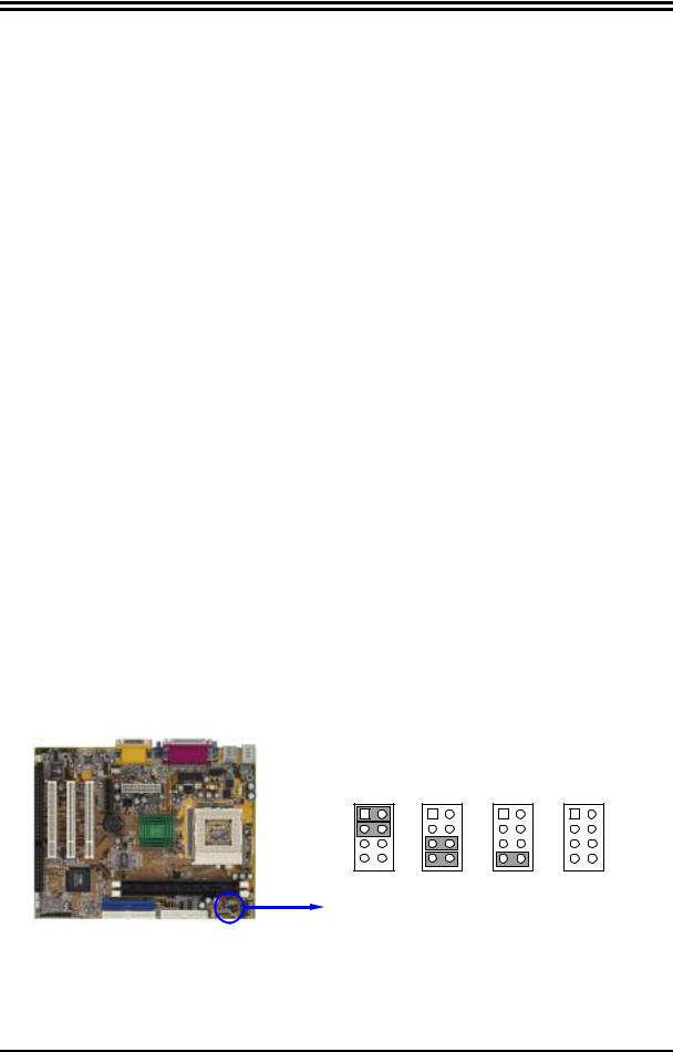
(1) CPU F.S.B. Clock setting: JMP1
The motherboard’s CPU Front Side Bus clock adjusted through jumper JPM1. This motherboard is jumper-less design. When you set JMP1 to AUTO, no jumper or switch are needed, you can then set CPU Frequency through the BIOS setup.
BIOS Setup>Miscellaneous Control>Host clock at Next Boot is
Table as below:
CPU (MHz) |
1-2 |
3-4 |
5-6 |
7-8 |
* Default |
AUTO |
ON |
ON |
OFF |
OFF |
|
66 MHz |
OFF |
OFF |
ON |
ON |
|
100 MHz |
OFF |
OFF |
OFF |
ON |
|
133 MHz |
OFF |
OFF |
OFF |
OFF |
|
|
JMP1 |
JMP1 |
JMP1 |
JMP1 |
1 |
1 |
1 |
|
1 |
4 |
4 |
4 |
|
4 |
AUTO 66MHz 100MHz 133MHz
CPU F.S.B. Clock Setting
(2) CMOS RAM Clear (3-pin): JBAT1
A battery must be used to retain the motherboard configuration in CMOS RAM short 1-2 pins of JBAT1 to store the CMOS data.
7
To clear the CMOS, follow the procedure below:
1.Turn off the system and unplug the AC power
2.Remove ATX power cable from ATX power connector
3.Locate JBAT1 and short pins 2-3 for a few seconds
4.Return JBAT1 to its normal setting by shorting pins 1-2
5.Connect ATX power cable back to ATX power connector
Note: When should clear CMOS
1.Troubleshooting
2.Forget password
3.After over clocking system boot fail
JBAT1 |
JBAT1 |
||||||||
1 |
|
|
|
|
1 |
|
|
|
|
|
|
|
|
|
|
|
|
||
3 |
|
|
|
|
3 |
|
|
|
|
|
|
|
|
|
|
|
|
||
|
|
|
|
|
|
|
|
|
|
1-2 closed Normal |
2-3 closed Clear CMOS |
||||||||
CMOS RAM Clear Setting
2-3 Install CPU
2-3-1 About Pentium III & Celeron™ 370-pin CPU
This motherboard supports both Pentium III & Celeron 370 pins CPU.
The way to recognize the specification of CPU from the packing Pentium III 370 pins FC-PGA
On the surface of the CPU as shown on the right picture, under the word of “PENTIUM III” the code is:
RB 80526 P2 866 256
RB : FC–PGA packing
P2 : P2–133MHz front side bus frequency PY–100MHz front side bus frequency 866 : CPU internal frequency, where here is
866MHz
256 : the size of L2 cache, where here is 256K
Celeron FC–PGA
On the surface of the CPU as shown on the right picture, under the word of “Celeron” the code is:
8

566/128/66/1.5V
566 : CPU internal frequency, where here is 566MHz 128 : the size of L2 cache, where here is 128K
66 : front side bus frequency, where here is 66MHz 1.5V : the voltage for the CPU
2-3-2 Setting CPU Bus Clock Jumper
Setting the CPU Front Side Bus Frequency
The motherboard uses jumper JMP1 for the front side bus frequency setting as shown from the table below:
CPU (MHz) |
1-2 |
3-4 |
5-6 |
7-8 |
* Default |
AUTO |
ON |
ON |
OFF |
OFF |
|
66 MHz |
OFF |
OFF |
ON |
ON |
|
100 MHz |
OFF |
OFF |
OFF |
ON |
|
133 MHz |
OFF |
OFF |
OFF |
OFF |
|
Example: Using a Pentium III 866 CPU with front side bus frequency of 133MHz and
PC-133 SDRAM module, the setting of JPM1 will be all OFF. Will form CPU BUS CLOCK be 133MHz.
For experience user looking for over clocking, please refer to sec 2-3-4
2-3-3 Install CPU
This motherboard provides a ZIF socket 370. The CPU that comes with the motherboard should have a cooling FAN attached to prevent overheating. If this is not the case, then purchase a correct cooling FAN before you turn on your system.
WARNING! Be sure that there is sufficient air circulation across the processor’s heatsink and CPU cooling FAN is working correctly, otherwise it may cause the processor and motherboard overheat and damage, you may install an auxiliary cooling FAN, if necessary.
To install a CPU, first turn off your system and remove its cover. Locate the ZIF socket and open it by first pulling the level sideways away from the socket then upward to a 90-degree angle. Insert the CPU with the correct orientation as shown below. The notched corner should point toward the end of the level. Because the CPU
9
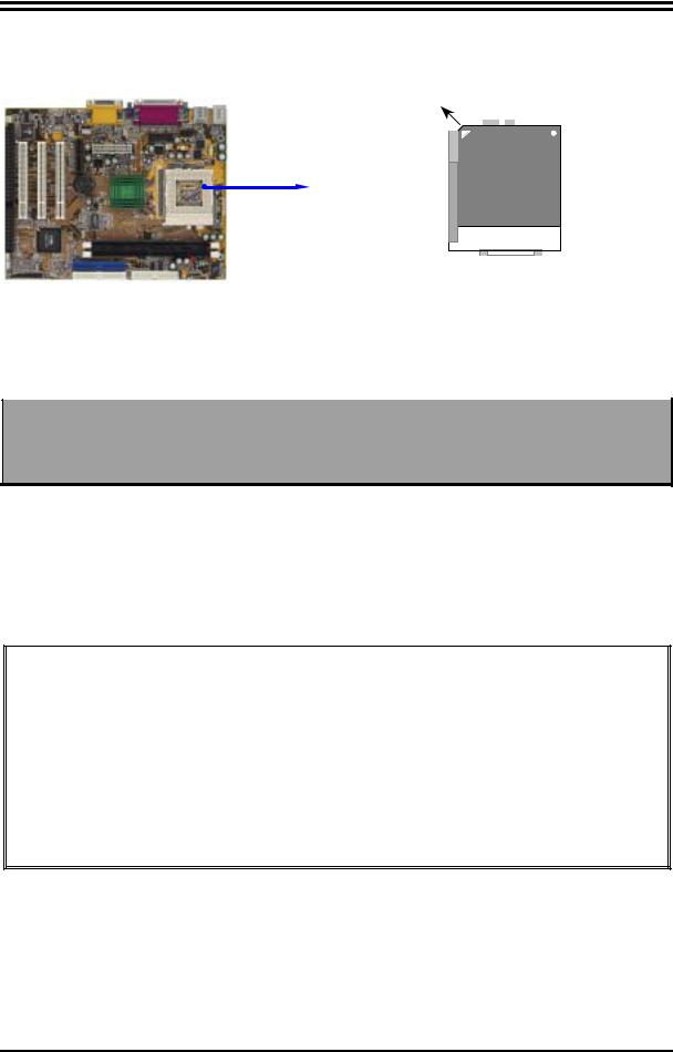
has a corner pin for two of the four corners, the CPU will only fit in the orientation as shown.
Colden Arrow
Pentium III
Intel
Socket 370
CPU ZIF Socket 370
When you put the CPU into the ZIF socket. No forces require to insert of the CPU, then press the level to locate position slightly without any extra force.
2-3-4 Over clock Running
WARNING! This section is for experienced motherboard installer only. Over clocking can result in system instability or even shortening life of the processor.
After setting the Jumper JMP1 you can choose over clock running by BIOS CMOS SETUP UTILITY. When you entered CMOS SETUP UTILITY, choose “Miscellaneous Control” you will see the screen as below then.
You can choose the situation you want to try.
CMOS Setup Utility – Copyright(C) 1984-2001 Award Software
Miscellaneous Control
CyrixIII Clock Ratio |
|
|
|
|
Default |
Item Help |
|||
Auto Detect DIMM/PCI Clock |
Enabled |
|
||
Spread Spectrum |
Disabled |
Menu Level > |
||
** Current Host Clock is 66MHz ** |
||||
Host Clock at Next Boot is |
[66MHz/33MHz] |
|
||
** Current DRAM Clock is 66Mhz ** |
|
|||
DRAM Clock at Next Boot is |
[66]MHz |
|
||
|
|
|
|
|
↑↓→←:Move Enter:Select +/-/PU/PD:Value F10:Save ESC:Exit F1:General Help
F5:Previous Values F6:Optimized Defaults F7:Standard Defaults
In “Host Clock at Next Boot is” item you can step by step change CPU Host Clock to approach over clocking.
2-4 Install Memory
10
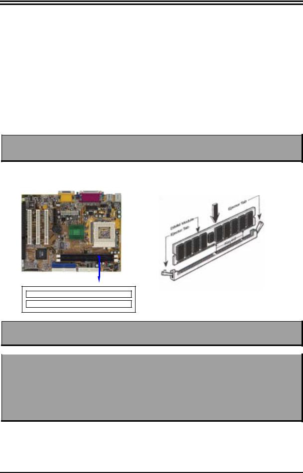
This motherboard provides two 168-pin DUAL INLINE MEMORY MODULES (DIMM) sites for memory expansion available from minimum memory size over 32MB to maximum memory size of 1GB SDRAM.
Valid Memory Configurations
DIMM1 |
DIMM2 |
System Accept or Not |
Total Memory |
||
Min. Max. |
|||||
|
|
|
|
||
DS/SS |
|
|
Accept |
32MB 512MB |
|
|
DS/SS |
|
Accept |
32MB 512MB |
|
DS/SS |
DS/SS |
|
Accept |
32MB 1GB |
|
DS : Double Sided DIMM |
SS : Single Sided DIMM |
||||
NOTE! Make sure the total installed memory does not exceeds 1GB, otherwise the system may hang during startup.
Generally, installing SDRAM modules to your motherboard is very easy, you can refer to figure 2-4 to see what a 168-Pin PC100 & PC133 SDRAM module looks like.
Figure 2-4
DIMM1 (BANK0+BANK1)
DIMM2 (BANK2+BANK3)
NOTE! When you install DIMM module fully into the DIMM socket the eject tab should be locked into the DIMM module very firmly and fit into its indention on both sides.
WARNING! If the SDRAM CLOCK is set at 133MHz, you must use only PC133compliant DIMMs. When this motherboard operate at 133Mhz, most system will not even boot if non-compliant SDRAM modules are used because of the strict timing issues, if your DIMM are not PC133compliant, set the SDRAM clock to 100MHz to ensure system’s stability.
2-5 Expansion Cards
11
 Loading...