


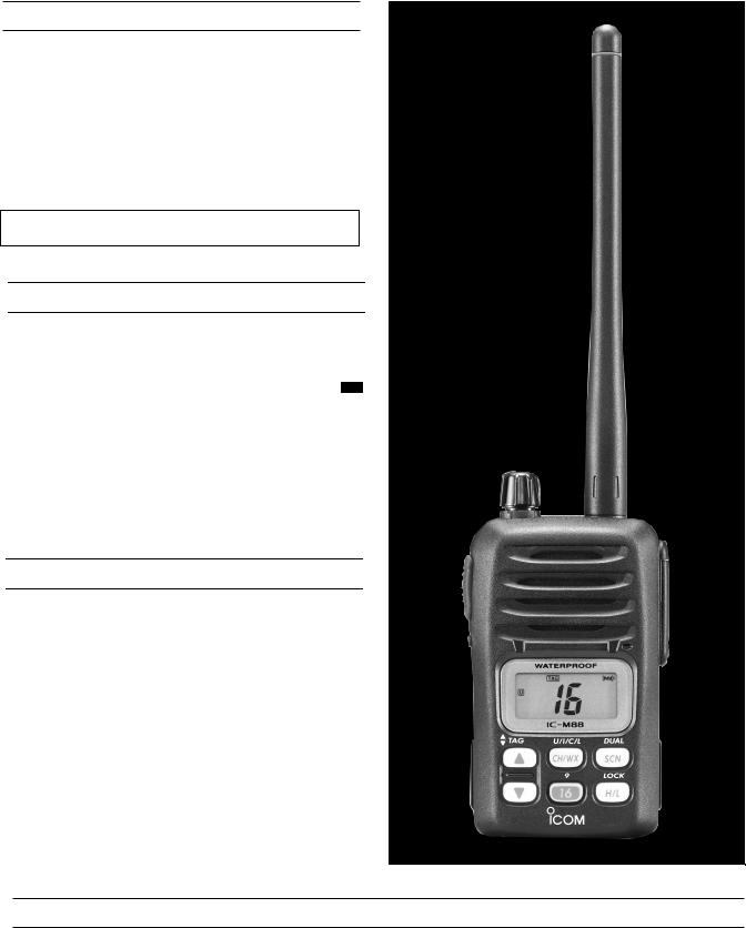
 Loading...
VHF MARINE TRANSCEIVER
iCm88
INTRODUCTION
This service manual describes the latest service information for the IC-M88 VHF MARINE TRANSCEIVER at the time of publication.
Model |
Version |
Symbol |
FM I/S |
Battery pack |
||
|
|
|
|
|
|
|
|
|
U.S.A. |
USA |
NO |
BP-227 |
|
IC-M88 |
|
|
|
|||
USA-1 |
YES |
BP-227FM |
||||
|
||||||
|
|
|
|
|
|
|
|
|
S.E. Asia |
SEA |
NO |
BP-227 |
|
|
|
|
|
|
|
|
To upgrade quality, all electrical or mechanical parts and internal circuits are subject to change without notice or obligation.
DANGER
NEVER connect the transceiver to an AC outlet or a DC power supply that uses more than 8.3 V. This will ruin the transceiver.
DO NOT expose the transceiver to rain, snow or liquids.
DO NOT reverse the polarities of the power supply  connecting the transceiver.
DO NOT apply an RF signal of more than 20 dBm (100 mW) to the antenna connector. This could damage the transceiverís front end.
ORDERING PARTS
Be sure to include the following four points when ordering replacement parts:
1.10-digit order numbers
2.Component part number and name
3.Equipment model name and unit name
4.Quantity required
<SAMPLE ORDER>
1110002750 |
S.IC TA7S01F |
IC-M88 |
MAIN UNIT |
1 piece |
8210019100 |
2600 Front panel |
IC-M88 |
CHASSIS |
5 pieces |
Addresses are provided on the inside back cover for your convenience.
REPAIR NOTES
1.Make sure the problem is internal before disassembling the transceiver.
2.DO NOT open the transceiver until the transceiver is disconnected from its power source.
3.DO NOT force any of the variable components. Turn them slowly and smoothly.
4.DO NOT short any circuits or electronic parts. An insulated tuning tool MUST be used for all adjustments.
5.DO NOT keep power ON for a long time when the transceiver is defective.
6.DO NOT transmit power into a signal generator or a sweep generator.
7.ALWAYS connect a 40 dB or 50 dB attenuator between the transceiver and a deviation meter or spectrum analyzer when using such test equipment.
8.READ the instructions of test equipment thoroughly before connecting equipment to the transceiver.

TABLE OF CONTENTS
SECTION |
1 |
SPECIFICATIONS |
|
SECTION |
2 |
INSIDE VIEWS |
|
SECTION |
3 |
DISASSEMBLY INSTRUCTIONS |
|
SECTION |
4 |
CIRCUIT DESCRIPTION |
|
|
4 - 1 |
RECEIVER CIRCUITS ................................................................................................... |
4 - 1 |
|
4 - 2 |
TRANSMITTER CIRCUITS ............................................................................................ |
4 - 2 |
|
4 - 3 |
PLL CIRCUITS................................................................................................................. |
4 - 3 |
|
4 - 4 |
POWER SUPPLY CIRCUITS ......................................................................................... |
4 - 3 |
|
4 - 5 |
CPU PORT ALLOCATIONS ........................................................................................... |
4 - 4 |
SECTION |
5 |
ADJUSTMENT PROCEDURES |
|
|
5 - 1 |
PREPARATION................................................................................................................ |
5 - 1 |
|
5 - 2 |
SOFTWARE ADJUSTMENT ........................................................................................... |
5 - 4 |
SECTION |
6 |
PARTS LIST |
|
SECTION |
7 |
MECHANICAL PARTS AND DISASSEMBLY |
|
SECTION |
8 |
SEMI-CONDUCTOR INFORMATION |
|
SECTION |
9 |
BOARD LAYOUTS |
|
|
9 - 1 |
CHARGER UNIT ............................................................................................................. |
9 - 1 |
|
9 - 2 |
VR UNIT .......................................................................................................................... |
9 - 1 |
|
9 - 3 |
CONNECTOR UNIT ........................................................................................................ |
9 - 1 |
|
9 - 4 |
MAIN UNIT....................................................................................................................... |
9 - 2 |
|
9 - 5 |
LOGIC UNIT .................................................................................................................... |
9 - 4 |
SECTION |
10 |
BLOCK DIAGRAM |
|
SECTION |
11 |
VOLTAGE DIAGRAM |
|

SECTION 1 SPECIFICATIONS
GENERAL
• Frequency coverage |
: TX: 156.025–157.425 MHz, RX: 156.050–163.275 MHz |
[MARINE] |
||
|
TX/RX: 146.000–174.000 MHz |
|
[LMR] |
|
• Number of free channels |
: 22 channels |
|
|
|
• Type of emission |
: 16K0G3E (Wide; 25 kHz) |
|
[MARINE] |
|
|
16K0F3E (Wide; 25 kHz), 8K50F3E (Narrow; 12.5 kHz) |
[LMR] |
||
• Antenna connector |
: SMA (50 Ω) |
|
|
|
• Power supply requirement |
: BP-227/FM (7.2 V DC, negative ground) |
|
||
• Current drain (approx.) |
: Transmit |
at High (5.0 W) |
1.6 A |
|
|
|
at Middle (3.0 W) |
1.2 A |
|
|
|
at Low1 (1.0 W) |
0.7 A |
|
|
Receive |
at maximum audio |
200 mA |
|
|
|
at stand-by |
Less than 120 mA |
|
• Usable temperature range |
: –20˚C to +60˚C; –4˚F to +140˚F |
|
[MARINE] |
|
|
–30˚C to +60˚C; –22˚F to +140˚F |
|
[LMR] |
|
• Dimensions (projections not included) : 62(W) × 97(H) × 39(D) mm; 27⁄16(W) × 313⁄16(H) × 117⁄32(D) in. |
|
|||
• Weight (with antenna, BP-227/FM) |
: 280 g; 97⁄8 oz (approx.) |
|
|
|
TRANSMITTER
• RF output power (with BP-227/FM) |
: 5 W / 3 W / 1 W (High / Middle / Low) |
|
|
• Modulation system |
: Variable reactance frequency modulation |
|
|
• Maximum frequency deviation |
: ±5.0 kHz (Wide) |
[MARINE] |
|
|
±5.0 kHz (Wide), ±2.5 kHz (Narrow) |
[LMR] |
|
• Frequency error |
: ±5.0 ppm |
|
|
• Spurious emissions |
: –70 dBc |
|
|
• Adjacent channel power |
: 70 dB |
|
[MARINE] |
|
70 dB (Wide), 60 dB (Narrow) |
[LMR] |
|
• Audio harmonic distortion |
: 10% at 60% deviation |
|
|
• FM Hum and noise |
: 40 dB |
|
[MARINE] |
|
40 dB (Wide), 34 dB (Narrow) |
[LMR] |
|
• Limiting charact modulation |
: 60–100% of maximum deviation |
|
|
• Ext. microphone connector |
: 9-pin multi connector/2.2 kΩ |
|
|
RECEIVER |
|
|
|
• Receive system |
: Double conversion superheterodyne system |
|
|
• Intermediate frequencies |
: 1st |
31.05 MHz |
|
|
2nd |
450 kHz |
|
• Sensitivity |
: 0.25 µV typical at 12 dB SINAD |
|
|
• Squelch sensitivity |
: 0.35 µV typical at threshold |
|
|
• Adjacent channel selectivity |
: 70 dB typical |
[MARINE] |
|
|
70 dB typical (Wide), 60 dB typical (Narrow) |
[LMR] |
|
• Spurious response rejection |
: 70 dB typical |
|
|
• Intermodulation rejection ratio |
: 70 dB typical |
|
|
• Hum and noise |
: 40 dB |
|
[MARINE] |
|
40 dB (Wide), 34 dB (Narrow) |
[LMR] |
|
• Audio output power (at 7.2 V DC) |
: 350 mW typical at 10% distortion with an 8 Ω load |
|
|
• Ext. speaker connector |
: 9-pin multi connector/8 Ω |
|
|
Specifications are measured in accordance with TIA/EIA-603.
All stated specifications are subject to change without notice or obligation.
1 - 1
VHF MARINE CHANNEL LIST
Channel No. |
Frequency (MHz) |
Channel No. |
Frequency (MHz) |
Channel No. |
Frequency (MHz) |
|||||||||
USA |
INT |
CAN |
Transmit |
Receive |
USA |
INT |
CAN |
Transmit |
Receive |
USA |
INT |
|
Transmit |
Receive |
|
01 |
01 |
156.050 |
160.650 |
21A |
|
21A |
157.050 |
157.050 |
73 |
73 |
|
156.675 |
156.675 |
|
|
|
|
|
|
|
|
|
|
|
|
|
|
|
01A |
|
|
156.050 |
156.050 |
|
22 |
|
157.100 |
161.700 |
74 |
74 |
|
156.725 |
156.725 |
|
|
|
|
|
|
|
|
|
|
|
|
|
|
|
|
02 |
02 |
156.100 |
160.700 |
22A |
|
22A |
157.100 |
157.100 |
77*1 |
77 |
|
156.875 |
156.875 |
|
03 |
03 |
156.150 |
160.750 |
|
23 |
23 |
157.150 |
161.750 |
|
78 |
|
156.925 |
161.525 |
|
|
|
|
|
|
|
|
|
|
|
|
|
|
|
03A |
|
|
156.150 |
156.150 |
23A |
|
|
157.150 |
157.150 |
78A |
|
|
156.925 |
156.925 |
|
|
|
|
|
|
|
|
|
|
|
|
|
|
|
|
04 |
|
156.200 |
160.800 |
24 |
24 |
24 |
157.200 |
161.800 |
|
79 |
|
156.975 |
161.575 |
|
|
|
|
|
|
|
|
|
|
|
|
|
|
|
|
|
04A |
156.200 |
156.200 |
25 |
25 |
25 |
157.250 |
161.850 |
79A |
|
|
156.975 |
156.975 |
|
|
|
|
|
|
|
|
|
|
|
|
|
|
|
|
05 |
|
156.250 |
160.850 |
26 |
26 |
26 |
157.300 |
161.900 |
|
80 |
|
157.025 |
161.625 |
|
|
|
|
|
|
|
|
|
|
|
|
|
|
|
05A |
|
05A |
156.250 |
156.250 |
27 |
27 |
27 |
157.350 |
161.950 |
80A |
|
|
157.025 |
157.025 |
|
|
|
|
|
|
|
|
|
|
|
|
|
|
|
06 |
06 |
06 |
156.300 |
156.300 |
28 |
28 |
28 |
157.400 |
162.000 |
|
81 |
|
157.075 |
161.675 |
|
|
|
|
|
|
|
|
|
|
|
|
|
|
|
|
07 |
|
156.350 |
160.950 |
|
60 |
60 |
156.025 |
160.625 |
81A |
|
|
157.075 |
157.075 |
|
|
|
|
|
|
|
|
|
|
|
|
|
|
|
07A |
|
07A |
156.350 |
156.350 |
|
61 |
|
156.075 |
160.675 |
|
82 |
|
157.125 |
161.725 |
|
|
|
|
|
|
|
|
|
|
|
|
|
|
|
08 |
08 |
08 |
156.400 |
156.400 |
61A |
|
61A |
156.075 |
156.075 |
82A |
|
|
157.125 |
157.125 |
|
|
|
|
|
|
|
|
|
|
|
|
|
|
|
09 |
09 |
09 |
156.450 |
156.450 |
|
62 |
|
156.125 |
160.725 |
|
83 |
|
157.175 |
161.775 |
|
|
|
|
|
|
|
|
|
|
|
|
|
|
|
10 |
10 |
10 |
156.500 |
156.500 |
|
|
62A |
156.125 |
156.125 |
83A |
|
|
157.175 |
157.175 |
|
|
|
|
|
|
|
|
|
|
|
|
|
|
|
11 |
11 |
11 |
156.550 |
156.550 |
|
63 |
|
156.175 |
160.775 |
84 |
84 |
|
157.225 |
161.825 |
|
|
|
|
|
|
|
|
|
|
|
|
|
|
|
12 |
12 |
12 |
156.600 |
156.600 |
63A |
|
|
156.175 |
156.175 |
84A |
|
|
157.225 |
157.225 |
|
|
|
|
|
|
|
|
|
|
|
|
|
|
|
13*2 |
13 |
13*1 |
156.650 |
156.650 |
|
64 |
64 |
156.225 |
160.825 |
85 |
85 |
|
157.275 |
161.875 |
14 |
14 |
14 |
156.700 |
156.700 |
64A |
|
64A |
156.225 |
156.225 |
85A |
|
|
157.275 |
157.275 |
|
|
|
|
|
|
|
|
|
|
|
|
|
|
|
15*2 |
15*1 |
15*1 |
156.750 |
156.750 |
|
65 |
|
156.275 |
160.875 |
86 |
86 |
|
157.325 |
161.925 |
16 |
16 |
16 |
156.800 |
156.800 |
65A |
65A |
65A |
156.275 |
156.275 |
86A |
|
|
157.325 |
157.325 |
|
|
|
|
|
|
|
|
|
|
|
|
|
|
|
17*1 |
17 |
17*1 |
156.850 |
156.850 |
|
66 |
|
156.325 |
160.925 |
87 |
87 |
|
157.375 |
161.975 |
|
18 |
|
156.900 |
161.500 |
66A |
66A |
|
156.325 |
156.325 |
87A |
|
|
157.375 |
157.375 |
|
|
|
|
|
|
|
|
|
|
|
|
|
|
|
18A |
|
18A |
156.900 |
156.900 |
67*2 |
67 |
|
156.375 |
156.375 |
88 |
88 |
|
157.425 |
162.025 |
|
19 |
|
156.950 |
161.550 |
68 |
68 |
|
156.425 |
156.425 |
88A |
|
|
157.425 |
157.425 |
|
|
|
|
|
|
|
|
|
|
|
|
|
|
|
19A |
|
19A |
156.950 |
156.950 |
69 |
69 |
|
156.475 |
156.475 |
|
|
|
|
|
|
|
|
|
|
|
|
|
|
|
|
|
|
|
|
20 |
20 |
20*1 |
157.000 |
161.600 |
70*3 |
70*3 |
|
156.525 |
156.525 |
|
|
|
|
|
20A |
|
|
157.000 |
157.000 |
71 |
71 |
|
156.575 |
156.575 |
|
|
|
|
|
|
|
|
|
|
|
|
|
|
|
|
|
|
|
|
|
21 |
21 |
157.050 |
161.650 |
72 |
72 |
|
156.625 |
156.625 |
|
|
|
|
|
|
|
|
|
|
|
|
|
|
|
|
|
|
|
|
*1 Low power only, *2 Momentary high power, *3 Receive only
NOTE: Channels 3, 21, 23, 61, 64, 81, 82 and 83 CANNOT be used by the general public in USA waters.
WX CHANNEL LIST
Weather |
Frequency (MHz) |
Weather |
Frequency (MHz) |
||
channel |
Transmit |
Receive |
channel |
Transmit |
Receive |
|
|
|
|
|
|
WX01 |
Receive only |
162.550 |
WX06 |
Receive only |
162.500 |
|
|
|
|
|
|
WX02 |
Receive only |
162.400 |
WX07 |
Receive only |
162.525 |
|
|
|
|
|
|
WX03 |
Receive only |
162.475 |
WX08 |
Receive only |
161.650 |
|
|
|
|
|
|
WX04 |
Receive only |
162.425 |
WX09 |
Receive only |
161.775 |
|
|
|
|
|
|
WX05 |
Receive only |
162.450 |
WX10 |
Receive only |
163.275 |
|
|
|
|
|
|
1 - 2

SECTION 2 INSIDE VIEWS
• LOGIC UNIT
Bottom view
*: Located in another side of this point.
|
|
|
|
|
|
|
AF mute circuit |
|
|
|
|
|
|
|
|
Q441* |
: 2SC4116 |
|
|
|
|
|
|
|
Q442* |
: CPH3403 |
IN/EXT microphone switch |
|
|
|
|
Q443 |
: CPH3403 |
||
|
|
|
|
Q444 |
: DTC144EU |
|||
(Q461, Q462: UN911H) |
|
|
|
|
|
|||
|
|
|
|
|
EEPROM |
|||
|
|
|
|
|
|
|
||
|
|
|
|
|
|
|
||
Microphone amplifier |
|
|
|
|
(IC591*: HN58X2416TI) |
|||
(IC471: NJM2904V) |
|
|
|
|
|
|
|
|
|
|
|
|
|
|
|
|
|
CPU
AF mute  (IC661: µPD780316GC-511-9EB) (IC481: TC4W66FU)
S5V regulator (Q561: 2SA1588)
M5V regulator
Q551: 2SB1132
Q552: XP6501
Q553: DTC144EU
• MAIN UNIT
Top view |
Bottom view |
Antenna switching circuit
D131, D151: 1SV307
D152: MA77
RF amplifier (Q165: 3SK294)
Power amplifier (Q111: RD07MVS1)
Pre-drive amplifier (Q101: RD01MUS1)
T5V regulator |
(Q323: 2SA1588) |
R5V regulator |
(Q322: 2SA1588) |
V5V regulator (Q321: 2SA1588)
VCO circuit
1st Mixer (Q191: 3SK299)
AF mute
(IC281: TC4W66FU)
APC control (IC141: TA75S01F)
Bandpass filter (FI211: FL-355)
PLL IC
(IC1: MB15A02PFV)
Reference frequency |
crystal |
(X1: CR664A; |
15.300 MHz) |
FM IF IC (IC231: TA31136FN)
IF amplifier (Q211: 2SC4215)
D/A converter (IC251:
M62363FP-650C)
2 - 1
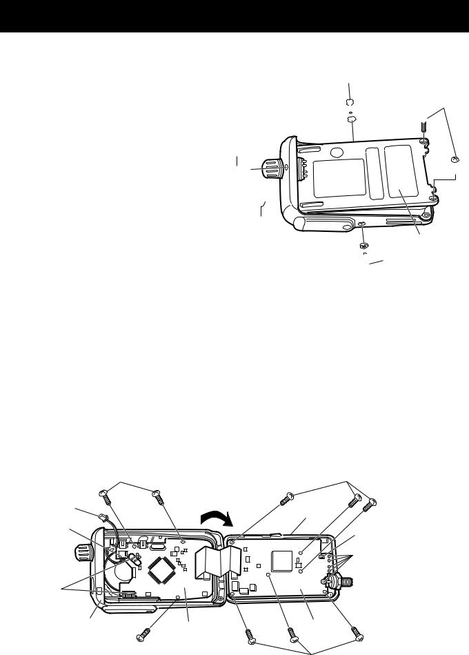
SECTION 3 DISASSEMBLY INSTRUCTIONS
1. Removing the chassis panel
q Remove nut A.
w Unscrew 2 screws B (2 × 8 mm, black) and 3 screws C (2 × 4 mm, black) from the chassis.
e Take off the chassis in the direction of the arrow.
NOTE: * Tighten the screws in order of a number (q–y) when assembling.
C
w
q 


A
C
y B
B  e
e

 r
r
Chassis
t  C
C
2. Removing the LOGIC unit.
q Unplug the cable from J281 on the MAIN unit to separate the LOGIC unit
wSeparate the front panel from the chassis in the direction of the arrow.
eUnsolder 2 leads of the speaker and connector unit (9 points).
rUnscrew 3 screws D (2 × 4 mm, silver) to separate the front panel.
NOTE: * Tighten the screws in order of a number (z–c) when assembling.
3. Removing the MAIN unit
qUnsolder 4 leads of contact spring and antenna connector (1 point).
wUnscrew 6 screws D (2 × 4 mm, silver) to separate the chassis.
NOTE: * Tighten the screws in order of a number (q–y) when assembling.
|
D |
|
E |
|
z |
c |
w |
t |
r |
J281 |
|
|
|
|
|
|
Chassis |
|
|
|
|
|
|
|
VR unit |
|
|
|
|
W801 |
|
|
|
J281 |
|
|
|
|
Unsolder
(A contact spring
and antenna connector)
Unsolder
(A SP and connector unit)
Front panel |
LOGIC UNIT |
|
MAIN UNIT |
|
|
||
x |
e |
y |
q |
D |
|
|
|
|
|
|
E |
3 - 1

SECTION 4 CIRCUIT DESCRIPTION
4-1 RECEIVER CIRCUITS
4-1-1 ANTENNA SWITCHING CIRCUIT (MAIN UNIT)
The antenna switching circuit functions as a low-pass filter while receiving and as resonator circuit while transmitting. The circuit does not allow transmit signals to enter receiver circuits.
Received signals from the antenna connector pass through the low-pass filter (L131, L132, C131–C136) and antenna switching circuit (D151, D152). The filtered signals are then applied to the RF amplifier circuit (Q165).
4-1-2 RF AND 1ST MIXER CIRCUITS (MAIN UNIT)
The 1st mixer circuit converts the received signals to a fixed frequency of the 1st IF signal with a PLL output frequency. By changing the PLL frequency, only the desired frequency will be passed through a pair of crystal filters at the next stage of the 1st mixer.
The signals from the antenna switching circuit are passed through the 2-stage bandpass filters (D154, D155, L154, L155) and amplified at the RF amplifier (Q165). The amplified signals are passed through another 2-stage bandpass filters (D181, D182, L181, L182), and then applied to the 1st mixer circuit (Q199).
The filtered signals are mixed at the 1st mixer (Q199) with a 1st LO signal coming from the PLL circuit to produce a 31.05 MHz 1st IF signal. The 1st IF signal is passed through a pair of crystal filter (FI211) and is then amplified at the IF amplifier (Q211).
4-1-3 2ND IF AND DEMODULATOR CIRCUITS (MAIN UNIT)
The 2nd mixer circuit converts the 1st IF signal to a 2nd IF signal. A double conversion superheterodyne system (which converts receive signal twice) improves the image rejection and obtain stable receiver gain.
• 2ND IF AND DEMODULATOR CIRCUITS
The 1st IF signal is applied to a 2nd mixer section of the FM IF IC (IC231, pin 16). The signal is then mixed with a 2nd LO signal for conversion into a 450 kHz 2nd IF signal.
IC231 contains the 2nd mixer, limiter amplifier, quadrature detector and active filter circuits. A 30.6 MHz 2nd LO signal is produced at the PLL circuit using the reference frequency.
The 2nd IF signal from the 2nd mixer (IC231, pin 3) passes through ceramic filters (FI231, FI232) to remove unwanted heterodyned frequencies. It is then amplified at the limiter amplifier section (IC231, pin 5) and applied to the quadrature detector section (IC231, pins 10 and 11) to demodulate the 2nd IF signal into AF signals.
4-1-4 AF CIRCUIT (MAIN AND LOGIC UNITS)
AF signals from the FM IF IC (IC231, pin 9) are fed to the analog switch (IC282).
The AF signals (detected signals) passes through the AF mute switch (IC281A, pins 2 and 1) via “DET” signal, and are then applied to the analog switch (IC282, pin 1). The signals are then applied to the low-pass filter (IC261B, C266, C267, R270–R272).
The filtered AF signals are applied to and adjusted audio level at the [VOL] control (VR unit; R801) via the “VOLIN” signal. The level controlled signals are passed through the AF mute switch (LOGIC unit; Q411) which is controlled by “AFMS” signal from the CPU (IC661, pin 84). The passed signals are applied to the AF power amplifier (IC421, pin 4), and then output to the internal speaker or [EXT SP] jack after being passed through the de-emphasis circuit (R411, C413) to obtain the –6 dB/octave frequency characteristics
R240  R241
R241
"SQCON" signal to the D/A convertor IC (IC251, pin 2)
|
|
|
Q231 |
2nd IF filters |
|
|
|
Q232 |
|
|
|
|
450 kHz |
|
|
|
|
W/N |
|
C238 |
C239 |
|
|
|
|
SW |
|
||
|
|
|
|
|
8 |
R239 |
7 |
5 |
Fl232 Fl231 |
|
|
|
Noise |
|
Active |
|
|
detector |
|
filter |
|
|
IF amp. |
|
|
|
|
|
|
FM |
|
|
|
|
|
"SQLOUT" signal to the D/A |
detector |
|
|
|
|
Noise |
convertor IC (IC251, pin 1) |
|
RSSI |
|
|||
|
|
comp. |
||||
|
|
|||||
|
|
|
|
|
|
|
C242 |
|
9 |
10 |
11 |
12 |
|
|
|
|
|
|
AF signal "DET" |
R242 |
|
|
C232 |
|
C244 |
|
|
|||
C243 |
|
R231 |
|
||
|
30.6 MHz |
|
|
|
|
|
|
|
2 |
17 |
16 |
||
|
|
|||||
3 |
2 Q221 |
PLL IC |
||||
|
|
|
|
IC1 |
||
2nd |
|
|
|
|
|
|
|
|
|
|
|
|
|
|
|
|
|
|
|
|
|
|
|
|
|
|
|
Mixer |
|
|
|
|
|
|
|
|
|
X1 |
|||
|
|
|
|
|||
|
|
|
15.3 MHz |
|||
IC231 TA31136FN(D)
14  16
16
"IF" (1st IF signal: 31.05 MHz) from RF unit, Q211
 "NOISV" signal to the CPU (pin 32)
R232 |
"RSSIV" signal to the CPU (pin 33) |
R5V
X231
450 kHz
4 - 1
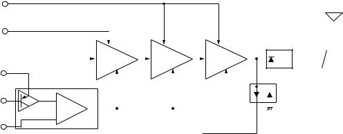
4-1-5 SQUELCH CIRCUIT (MAIN AND LOGIC UNITS)
The noise squelch circuit cuts out AF signals when no RF signals are received. By detecting noise components in the AF signals, the squelch circuit switches the AF mute switch.
A portion of the AF signals divided by C242 from the FM IF IC (IC231, pin 9) are applied to the D/A converter (IC251, pin 2) to adjust amplitude. The signals from the D/A converter (IC251, pin 1) are applied to the active filter section (IC231, pin 8, R239–R241, C237, C238). The active filter section amplifies and filters noise components. The filtered signals are applied to the noise detector section and output from IC231 (pin 14) as the “NOISV” signal.
The “NOISV” signal from IC231 (pin 14) is applied to the CPU (LOGIC unit; IC611, pin 32). The CPU compares the set squelch level voltage and “NOISV” signal voltage to control the squelch output.
4-2 TRANSMITTER CIRCUITS
4-2-1 MICROPHONE AMPLIFIER CIRCUIT (LOGIC AND MAIN UNITS)
The microphone amplifier circuit amplifies audio signals with +6 dB/octave pre-emphasis characteristics from the microphone to a level needed for the modulation circuit.
• In case of the internal microphone
The AF signals from the internal microphone (MC461) is applied to the microphone amplifier (IC471a, pin 6) via the “INMIC” signal.
• In case of external microphone
The AF signals from the external microphone (CP458) is applied to the microphone amplifier (IC471a, pin 6) via the “EXTMIC” signal.
The amplified signals are passed through the pre-emphasis circuit (R463, C463) and are then applied to the AF mute switch (IC481a, pin 1) via the “MICO” signal after being passed through the another microphone amplifier (IC471b, pins 2 and 1).
The AF signals are amplified again at the limiter-amplifier (IC491a, pin 2) and then passed through the low-pass filter (IC491b, pins 6 and 7). The filtered audio passes through the analog swtich (MAIN unit; IC251, pins 4 and 3), and is then applied to the MAIN unit as the “MOCON” signal.
4-2-2 MODULATION CIRCUIT (MAIN UNIT)
The modulation circuit modulates the VCO oscillating signal (RF signal) using the microphone audio signals.
The audio signals “MOCON” change the reactance of D39 to modulate an oscillated signal at the TX VCO circuit (Q51, D35–D38, L34, L51, C32, C33, C52–C54). The oscillated signal is amplified at the buffer-amplifiers (Q61, Q62).
4-2-3 PRE-DRIVE/POWER AMPLIFIER CIRCUITS (MAIN UNIT)
The signal from the VCO circuit passes through the transmit/receive switching circuit (D91, D92) and is applied to the buffer-amplifier (Q91). The amplified signal is amplified by the pre-driver (Q101) and the power amplifier (Q101) to obtain 5 W of RF power (at 7.2 V). The amplified signal passes through the antenna switching circuit (D131), and low-pass filter (L131, L132, C131–C136) and is then applied to the antenna connector.
The bias current of the buffer amplifier (Q91), pre-driver (Q101) and power amplifier (Q111) is controlled by the APC circuit to stabilize the output power.
4-2-4 APC CIRCUIT (MAIN UNIT)
The APC circuit provides stable output power from the power amplifier even when the input voltage or temperature changes, and, selects HIGH, MIDDLE, LOW or EXTRA LOW output power. The APC circuit consists of a power detector and APC control circuits.
• POWER DETECTOR CIRCUIT (MAIN UNIT)
The power detector circuit (D132) detects the transmit output power level and converts it to DC voltage as the “TDETV” signal. The detected signal is applied to the APC control circuit.
• APC CONTROL CIRCUIT (MAIN AND LOGIC UNITS)
The “TDETV” signal from the power detector circuit is applied to the CPU (LOGIC unit; IC661, pin 31) to control the input voltage of the buffer amplifier (Q91), pre-driver (Q101) and power amplifier (Q111). When the output power changes, the CPU (LOGIC unit; IC661) outputs APC control signal to the D/A converter (IC190). And then “T1CON” signal from the D/A converter controls the APC controller (IC141) to provide stable output power.
• APC CIRCUIT |
VCC |
|
|
|
T5V |
|
S5V |
"TXMS" signal from the expander IC (IC341, pin 12)
"T1CON" signal from the D/A convertor IC (IC251, pin 14)
antenna
RF signal |
|
Q91 |
|
Q101 |
|
|
Q111 |
|
|
|
|
|
|
D131 |
|
|
|||||||
|
|
|
|
|
|
|
|
|
|
|
|
||||||||||||
|
|
|
|||||||||||||||||||||
from PLL |
Buffer |
|
Pre-drive |
|
Power |
|
|
|
|
|
|
|
ANT |
|
|
||||||||
|
|
|
|
|
|
|
|
|
LPF |
|
|||||||||||||
|
|
|
|
amp. |
|
amp. |
|
amp. |
|
|
|
|
|
|
|
SW |
|
|
|||||
|
|
|
|
|
|
|
|
|
|
|
|
|
|
|
|||||||||
|
|
|
|
|
|
|
|
|
|
|
|
|
|
|
|||||||||
|
|
3 |
|
|
|
|
|
|
|
|
|
|
|
|
|
|
|
|
|
Power detector |
|||
|
|
|
|
|
|
|
|
|
|
|
|
|
|
|
|
|
|
|
|||||
|
|
|
|
|
|
|
|
|
|
|
|
|
|
|
|
|
|
|
|||||
|
|
|
|
|
|
|
|
|
|
|
|
|
|
|
|
|
|
|
|||||
|
|
|
|
|
|
|
|
|
|
|
|
|
|
|
|
|
|
|
circuit (D132) |
||||
|
|
|
|
|
|
|
|
|
|
|
|
|
|
|
|
|
|
|
|||||
|
|
|
|
|
|
|
|
|
|
|
|
|
|
|
|
|
|
|
|
||||
Q141 |
IC141 |
|
|
|
|
|
|
|
|
|
|
|
|
|
|
|
|
|
|
|
|
|
|
|
|
|
|
|
|
|
|
|
|
|
|
|
|
|
|
|
|
|
|
|
|||
|
|
1 |
|
|
|
|
|
|
|
|
|
|
|
|
|
|
|
|
|
|
|
|
|
APC control circuit
"TDETV" to the CPU  (LOGIC unit; IC661, pin 31)
4 - 2
4-3 PLL CIRCUIT (MAIN UNIT)
4-3-1 GENERAL
The PLL circuit provides stable oscillation of the transmit frequency and receive 1st LO frequency. The PLL output compares the phase of the divided VCO frequency to the reference frequency. The PLL output frequency is controlled by the divided ratio (N-data) of a programmable divider. IC1 is a PLL IC which controls both VCO circuit for TX and RX.
The PLL circuit, using a one chip PLL IC (IC1), directly generates the transmit frequency and receive 1st IF frequency with VCOs. The PLL sets the divided ratio based on serial data from the CPU on the LOGIC unit and compares the phases of VCO signals with the reference oscillator frequency. The PLL IC detects the out-of-step phase and output from the pin 6 for TX and RX. The reference frequency (15.3 MHz) is oscillated at X1.
4-3-2 TX AND RX LOOP CIRCUITS (MAIN UNIT)
The generated signal at the TX-VCO circuit (Q51, D35 –D38, L34, L51, C32, C33, C52–C54) or RX-VCO (Q41, D31–D34, L32, L41, C31, C41–C43) enters the PLL IC (IC1, pin 8) and is divided at the programmable divider section and is then applied to the phase detector section.
The phase detector compares the input signal with a reference frequency, and then outputs the out-of-phase signal (pulse-type signal) from pin 6.
The pulse-type signal is converted into DC voltage (lock voltage) at the loop filter (R17–R19, C16–C19), and then applied to varactor diodes (TX; D35–D38, RX; D31–D34) of the TX-VCO and RX-VCO to stabilize the oscillated frequency.
4-3-3 TX AND RX VCO CIRCUITS (MAIN UNIT)
The VCO circuit from Q41 (RX) and Q5 (TX) are buffer amplified at the Q61 and Q62, and then sent to the TX/RX swtich (D91, D92). The receive LO signal is applied to the 1st mixer circuit (Q191) through an attenuator (L203, R203 –R206, C202, C203), and the transmit signal is applied to the buffer amplifier (Q91). A portion of the VCO output is reapplied to the PLL IC (IC1, pin 8) via the Q71.
• PLL CIRCUIT
4-4 POWER SUPPLY CIRCUITS
VOLTAGE LINES
LINE |
DESCRIPTION |
|
|
|
|
HV |
The voltage from the attached battery pack. |
|
|
|
|
|
The same voltage as the HV line (battery |
|
|
voltage) which is controlled by the power switch |
|
|
(VR unit; [OFF/VOL] control). |
|
VCC |
The output voltage is applied to the pre-drive |
|
|
(MAIN unit; Q101), power amplifier (MAIN unit; |
|
|
Q111), CPU5V and M5V regulator circuits |
|
|
(LOGIC unit; IC551 and Q551–Q553). |
|
|
|
|
|
Common 5 V converted from the VCC line by the |
|
|
CPU5V regulator circuit (LOGIC unit; IC551). |
|
CPU5V |
The output voltage is applied to the CPU (LOGIC |
|
|
unit; IC661), RESET circuit (LOGIC unit; IC581), |
|
|
etc. |
|
|
|
|
|
Common 5V converted from the VCC line by the |
|
|
M5V regulator circuit (LOGIC unit; Q551–Q553). |
|
M5V |
The output voltage is applied to R5V, T5V, V5V and |
|
S5V regulator circuits (LOGIC unit; Q322, Q323, |
||
|
||
|
Q321 and Q561). |
|
|
|
|
|
Receive 5V converted from the M5V line by the |
|
|
R5V regulator circuit (MAIN unit; Q322). |
|
R5V |
The regulated voltage is applied to the 1st mixer |
|
|
circuit (MAIN unit; Q191), RF and IF amplifiers |
|
|
(MAIN unit; Q165, Q211). |
|
|
|
|
|
Transmit 5V converted from the M5V line by the |
|
T5V |
T5V regulator circuit (MAIN unit; Q222). |
|
The regulated voltage is applied to the buffer |
||
|
||
|
amplifier (MAIN unit; Q91). |
|
|
|
|
|
Common 5V converted from the M5V line by |
|
V5V |
the V5V regulator circuit (MAIN unit; Q321). |
|
The regulated voltage is applied to the ripple |
||
|
||
|
filter circuit (Q47). |
|
|
|
|
|
Common 5V converted from the M5V line by the |
|
|
S5V regulator circuit (LOGIC unit; Q561). |
|
S5V |
The regulated voltage is applied to the microphone |
|
amplifier (LOGIC unit; IC471), limit amplifier |
||
|
||
|
(LOGIC unit; IC491), LCD back light (LOGIC unit; |
|
|
DS651–DS654), etc. |
|
|
|
S5V
RX VCO
Q81
Q82
VCOS |
Q41, D31 D34 |
Buffer |
D91 to transmitter circuit |
|
|
|
|
Buffer |
Q62 |
|
to the 1st mixer circuit |
|
|
TX VCO |
|
|
|
||
|
|
|
|
|
|
||
VCO SWITCH |
|
|
|
Q61 |
Buffer |
|
D92 |
FM |
|
Q51, D35 D38 |
|
|
|
|
|
MOD. |
|
|
|
Q71 |
|
|
|
|
|
|
|
|
|
||
D39 |
|
|
|
|
|
|
|
Loop |
|
|
|
IC1 MB15A02PFV |
|
LPF |
|
filter |
|
|
|
|
|
|
|
|
|
|
|
|
|
|
|
|
5 |
Phase |
Programmable |
Prescaler |
8 |
|
|
|
|
detector |
counter |
|
|
|
|
"2nd LO" signal (30.6 MHz) |
|
|
|
|
|
||
|
|
|
|
|
11 |
PLSTBO |
|
to the FM IF IC (IC231, pin 2) |
2 |
Programmable |
|
|
|||
Shift register |
10 |
||||||
2 |
|
divider |
|
9 |
SDATAO |
||
Q221 |
|
|
|
|
SCLKO |
||
1 |
|
|
|
|
|
||
X1 |
|
|
|
|
|
|
|
15.3 MHz |
|
|
|
|
|
|
|
4 - 3
4-5 PORT ALLOCATIONS
4-5-1 CPU (LOGIC UNIT; IC661)
Pin |
Port |
|
Description |
|
||
number |
name |
|
|
|||
|
|
|
|
|||
|
|
|
|
|||
1 |
BEEP |
Outputs beep audio signals. |
|
|||
|
|
|
||||
2 |
VSSTB |
Outputs strobe signals for the scrambler |
||||
IC (MAIN unit; IC381, pin 10). |
|
|||||
|
|
|
||||
|
|
|
|
|||
3 |
EXSTB |
Outputs strobe signals |
for the |
|||
expander IC (MAIN unit; IC341, pin 1). |
||||||
|
|
|||||
|
|
|
|
|
||
4 |
DASTB |
Outputs strobe |
signals for |
the D/A |
||
converter (MAIN unit; IC251, pin 6). |
||||||
|
|
|||||
|
|
|
||||
5 |
PLSTB |
Outputs strobe signals for the PLL IC |
||||
(MAIN unit; IC1, pin 11). |
|
|||||
|
|
|
||||
|
|
|
|
|||
6 |
ERXDI |
Input port for cloning signals. |
|
|||
|
|
|
|
|||
7 |
ETXDO |
Outputs cloning signals. |
|
|||
|
|
|
||||
10 |
SDATA |
Outputs serial data for PLL, scrambler |
||||
ICs, etc. |
|
|
|
|||
|
|
|
|
|
||
|
|
|
||||
11 |
SCLK |
Outputs serial clock for PLL, |
||||
scrambler ICs, etc. |
|
|||||
|
|
|
||||
|
|
|
||||
12 |
ESCK |
Outputs clock signal for the EEPROM |
||||
(IC591, pin 6). |
|
|
||||
|
|
|
|
|||
|
|
|
||||
13 |
ESDA |
I/O port for EEPROM data signal |
||||
(IC591, pin 5). |
|
|
||||
|
|
|
|
|||
|
|
|
||||
17 |
CSIFT |
Outputs CPU clock shift signal. |
||||
High : While clock is shifted. |
|
|||||
|
|
|
||||
|
|
|
||||
27 |
WDECV |
Input port for the WX tone detection. |
||||
|
|
|
||||
28 |
WETIN |
Input port for the transceiver’s internal |
||||
inundation detection. |
|
|||||
|
|
|
||||
|
|
|
|
|
||
29 |
EXTSV |
Input port |
for the external |
terminal |
||
connecting detection. |
|
|||||
|
|
|
||||
|
|
|
|
|
|
|
30 |
BATTV |
Input port |
for |
the battery |
voltage |
|
detection. |
|
|
|
|||
|
|
|
|
|
||
|
|
|
|
|
||
31 |
TDETV |
Input port |
for |
transmit RF level |
||
detection. |
|
|
|
|||
|
|
|
|
|
||
|
|
|
||||
32 |
NOISV |
Input port for noise level detection. |
||||
|
|
|
|
|
||
33 |
RSSIV |
Input port |
for |
RSSI voltage level |
||
detection. |
|
|
|
|||
|
|
|
|
|
||
|
|
|
||||
34 |
LOINV |
Input port for VCO lock voltage level |
||||
detection. |
|
|
|
|||
|
|
|
|
|
||
|
|
|
||||
35 |
TEMPV |
Input port for the transceiver’s internal |
||||
temperature detection. |
|
|||||
|
|
|
||||
|
|
|
||||
36 |
CDECV |
Input port for CTCSS/DTCS detection. |
||||
|
|
|
|
|||
38 |
ATIS |
Outputs ATIS wave form. |
|
|||
|
|
|
|
|
|
|
46–48 |
COM0– |
Output LCD common signals |
|
|||
COM2 |
|
|||||
|
|
|
|
|
||
|
|
|
|
|
|
|
51–70 |
SEG0– |
Output LCD segment signals. |
|
|||
SEG19 |
|
|||||
|
|
|
|
|
||
|
|
|
|
|
|
|
75 |
CONT1 |
Output LCD contrast control signals. |
||||
76 |
CONT2 |
|||||
|
|
|
|
|||
|
|
|
||||
77 |
LEDS1 |
Output LCD and key’s back light |
||||
78 |
LEDS2 |
dimmer control signal. |
|
|||
|
|
|
|
|
|
|
Pin |
Port |
Description |
|
number |
name |
||
|
|||
|
STXMS |
Outputs scrambler mute signal for the |
|
79 |
AF mute circuit (IC481, pin 3). |
||
|
|||
|
|
Low : While scrambler is muting. |
|
|
|
|
|
|
|
Outputs mic mute signal for the AF |
|
80 |
MICMS |
mute circuit (IC481, pin 7). |
|
Low : While the microphone is |
|||
|
|
||
|
|
muting. |
|
|
|
|
|
|
|
Outputs the internal speaker control |
|
81 |
ISPMS |
signal. |
|
|
|
High : While the speaker is muting. |
|
|
|
|
|
82 |
LDTFS |
Outputs DTCS’s low-pass filter cut-off |
|
frequency control signal. |
|||
|
|
||
|
|
|
|
83 |
W/NS |
Outputs Wide/Narrow control signal. |
|
high : While Narrow is selected. |
|||
|
|
||
|
|
|
|
|
AFMS |
Outputs the AF mute circuit control |
|
84 |
signal. |
||
|
|
High : The AF mute circuit is ON. |
|
|
|
|
|
|
AFVS |
Outputs AF amplifier’s power supply |
|
85 |
control signal. |
||
|
|
High : The AF amplifier is ON. |
|
|
|
|
|
|
M5VS |
Outputs M5V power supply control |
|
86 |
signal. |
||
|
|
Low : The common 5V is supplied. |
|
|
|
|
|
|
S5VS |
Outputs S5V power supply control |
|
87 |
signal. |
||
|
|
Low : The common 5V is supplied. |
|
|
|
|
|
|
|
Outputs V5V power supply control |
|
88 |
V5VS |
signal. |
|
|
|
Low : The common 5V is supplied. |
|
|
|
|
|
|
R5VS |
Outputs R5V power supply control |
|
89 |
signal. |
||
|
|
Low : While receiving. |
|
|
|
|
|
|
T5VS |
Outputs T5V power supply control |
|
90 |
signal. |
||
|
|
Low : While transmitting. |
|
|
|
|
|
98 |
CENC1 |
|
|
99 |
CENC2 |
Output DTCS/CTCSS wave form. |
|
100 |
CENC3 |
|
|
|
|
|
|
102 |
PTTIN |
Input port for [PTT] swtich detection. |
|
High : While [PTT] switch is pushed. |
|||
|
|
||
|
|
|
|
|
|
Input port for HM-138 (optional |
|
|
|
speaker-microphone)’s [PTT] swtich |
|
103 |
EPTTIN |
detection. |
|
|
|
Low : While HM-138’s [PTT] switch |
|
|
|
is pushed. |
|
|
|
|
|
|
BTYPE |
Input port for the connecting battery |
|
104 |
type detection. |
||
|
|
Low : While using alkaline cells. |
|
|
|
|
|
109 |
SQL |
Input port for the [SQL] key. |
|
Low : While [SQL] key is pushed. |
|||
|
|
||
|
|
|
|
110 |
UP |
Input port for the [UP] key. |
|
Low : While [UP] key is pushed. |
|||
|
|
||
|
|
|
4 - 4
CPU–Continued
Pin |
Port |
|
Description |
|
number |
name |
|
||
|
|
|||
|
|
|
||
111 |
DOWN |
Input port for the [DOWN] key. |
||
Low |
: While [DOWN] key is pushed. |
|||
|
|
|||
|
|
|
||
112 |
CH/WX |
Input port for the [CH/WX] key. |
||
Low |
: While [CH/WX] key is pushed. |
|||
|
|
|||
|
|
|
||
113 |
16/9 |
Input port for the [16/9] key. |
||
Low |
: While [16/9] key is pushed. |
|||
|
|
|||
|
|
|
||
114 |
SCAN |
Input port for the [SCAN] key. |
||
Low |
: While [SCAN] key is pushed. |
|||
|
|
|||
|
|
|
||
115 |
H/L |
Input port for the [H/L] key. |
||
Low |
: While [H/L] key is pushed. |
|||
|
|
|||
|
|
|
||
119 |
UNLK |
Input port for the PLL unlock signal. |
||
High : PLL lock voltage is unlocked. |
||||
|
|
|||
|
|
|
|
|
4-5-2 EXPANDER IC (MAIN UNIT; IC341)
Pin |
Port |
Description |
|
number |
name |
||
|
|||
|
|
|
|
|
|
Outputs the AF mute switch (IC281, |
|
5 |
SRXMS |
pin 3) control signal. |
|
Low : While the scrambler decording |
|||
|
|
||
|
|
signal is muted. |
|
|
|
|
|
|
|
Outputs the AF mute swtich (IC281, |
|
6 |
DETMS |
pin 7) control signal.signal. |
|
|
|
Low : While AF signal is muted. |
|
|
|
|
|
|
|
Outputs the scrambler IC’s clock shift |
|
7 |
CKSIS |
control signal. |
|
|
|
High : While the clock is shifted. |
|
|
|
|
|
|
|
Outputs the RF attenuator control |
|
11 |
ATTS |
signal. |
|
|
|
High : While attenuator is ON. |
|
|
|
|
|
|
|
Outputs the TX mute swtich (Q141) |
|
12 |
TXMS |
control signal. |
|
|
|
Low : While receiving. |
|
|
|
|
|
13 |
VCOS |
Outputs the TX/RX VCO control |
|
signal. |
|||
|
|
||
|
|
|
4-5-3 D/A CONVERTOR IC (MAIN UNIT; IC251)
Pin |
Port |
Description |
|
||
number |
name |
|
|||
|
|
|
|||
|
|
|
|||
2 |
SQCON |
Outputs squelch level control signal. |
|||
|
|
|
|||
3 |
MOCON |
Outputs modulatin level control signal. |
|||
|
|
|
|||
10 |
DTCON |
Outputs DTCS modulation balance |
|||
control signal. |
|
|
|||
|
|
|
|
||
|
|
|
|
|
|
11 |
FRCON |
Outputs reference |
frequency |
level |
|
control signal. |
|
|
|||
|
|
|
|
||
|
|
|
|
|
|
14 |
T1CON |
Outputs bandpass |
filter1 tuned |
and |
|
transmitting power control signals. |
|||||
|
|
||||
|
|
|
|||
15 |
T2CON |
Outputs bandpass filter2 tuned signal. |
|||
|
|
|
|||
22 |
T3CON |
Outputs bandpass filter3 tuned signal. |
|||
|
|
|
|||
23 |
T4CON |
Outputs bandpass filter4 tuned signal. |
|||
|
|
|
|
|
|
4 - 5
Loading...