


 Loading...
MPB3021AT
MPB3032AT
MPB3043AT
MPB3052AT
MPB3064AT
DISK DRIVES
PRODUCT MANUAL
C141-E045-02EN

|
|
REVISION RECORD |
|
|
|
Edition |
Date published |
Revised contents |
|
|
|
01 |
August., 1997 |
|
|
|
|
02 |
March, 1998 |
All pages revised. |
|
|
|
|
|
|
Specification No.: C141-E045-**EN
The contents of this manual is subject to change without prior notice.
All Rights Reserved.
Copyright ã 1998 FUJITSU LIMITED
C141-E045-02EN |
i |
PREFACE
This manual describes the MPB3021AT/MPB3032AT/MPB3043AT/MPB3052AT/MPB3064AT, a 3.5-inch hard disk drive with a BUILT-IN controller that is compatible with the ATA interface.
This manual explains, in detail, how to incorporate the hard disk drives into user systems.
This manual assumes that users have a basic knowledge of hard disk drives and their application in computer systems.
This manual consists of the following six chapters:
Chapter 1 |
DEVICE OVERVIEW |
Chapter 2 |
DEVICE CONFIGURATION |
Chapter 3 |
INSTALLATION CONDITIONS |
Chapter 4 |
THEORY OF DEVICE OPERATION |
Chapter 5 |
INTERFACE |
Chapter 6 |
OPERATIONS |
In this manual, disk drives may be referred to as drives or devices.
C141-E045-02EN |
iii |

Conventions for Alert Messages
This manual uses the following conventions to show the alert messages. An alert message consists of an alert signal and alert statements. The alert signal consists of an alert symbol and a signal word or just a signal word.
The following are the alert signals and their meanings:
This indicates a hazarous situation likely to result in serious personal injury if the user does not perform the procedure correctly.
This indicates a hazarous situation could result in personal injury if the user does not perform the porocedure correctly.
This indicates a hazarous situation could result in minor or moderate personal injury if the user does not perform the procedure correctly. This alert signal also indicates that damages to the product or other property, may occur if the user does not perform the procedure correctly.
This indicates information that could help the user use the product more efficiently.
In the text, the alert signal is centered, followed below by the indented message. A wider line space precedes and follows the alert message to show where the alert message begins and ends. The following is an example:
(Example)
IMPORTANT
HA (host adapter) consists of address decoder, driver, and receiver. ATA is an abbreviation of "AT attachment". The disk drive is conformed to the ATA-3 interface
The main alert messages in the text are also listed in the “Important Alert Items.”
iv |
C141-E045-02EN |
LIABILITY EXCEPTION
"Disk drive defects" refers to defects that involve adjustment, repair, or replacement.
Fujitsu is not liable for any other disk drive defects, such as those caused by user misoperation or mishandling, inappropriate operating environments, defects in the power supply or cable, problems of the host system, or other causes outside the disk drive.
C141-E045-02EN |
v |
CONTENTS
|
|
|
page |
|
CHAPTER 1 |
DEVICE OVERVIEW ................................................................................... |
1 |
- 1 |
|
1.1 |
Features |
.......................................................................................................................... |
1 |
- 1 |
1.1.1 |
Functions and performance ............................................................................................ |
1 |
- 1 |
|
1.1.2 |
Adaptability .................................................................................................................... |
1 |
- 2 |
|
1.1.3 |
Interface.......................................................................................................................... |
1 |
- 2 |
|
1.2 |
Device Specifications ..................................................................................................... |
1 |
- 4 |
|
1.2.1 |
Specifications summary.................................................................................................. |
1 |
- 4 |
|
1.2.2 |
Model and product number ............................................................................................ |
1 |
- 5 |
|
1.3 |
Power Requirements....................................................................................................... |
1 |
- 5 |
|
1.4 |
Environmental Specifications ......................................................................................... |
1 |
- 8 |
|
1.5 |
Acoustic Noise ............................................................................................................... |
1 |
- 8 |
|
1.6 |
Shock and Vibration ....................................................................................................... |
1 |
- 9 |
|
1.7 |
Reliability ....................................................................................................................... |
1 |
- 9 |
|
1.8 |
Error Rate ....................................................................................................................... |
1 |
- 10 |
|
1.9 |
Media Defects................................................................................................................. |
1 |
- 10 |
|
CHAPTER 2 |
DEVICE CONFIGURATION ....................................................................... |
2 |
- 1 |
|
2.1 |
Device Configuration ..................................................................................................... |
2 |
- 1 |
|
2.2 |
System Configuration..................................................................................................... |
2 |
- 4 |
|
2.2.1 |
ATA interface ................................................................................................................. |
2 |
- 4 |
|
2.2.2 |
1 drive connection .......................................................................................................... |
2 |
- 4 |
|
2.2.3 |
2 drives connection......................................................................................................... |
2 |
- 5 |
|
CHAPTER 3 |
INSTALLATION CONDITIONS................................................................. |
3 |
- 1 |
|
3.1 |
Dimensions..................................................................................................................... |
3 |
- 1 |
|
3.2 |
Mounting ........................................................................................................................ |
3 |
- 3 |
|
3.3 |
Cable Connections.......................................................................................................... |
3 |
- 7 |
|
3.3.1 |
Device connector ............................................................................................................ |
3 |
- 7 |
|
3.3.2 |
Cable connector specifications ....................................................................................... |
3 |
- 8 |
|
3.3.3 |
Device connection .......................................................................................................... |
3 |
- 8 |
|
3.3.4 |
Power supply connector (CN1) ...................................................................................... |
3 |
- 9 |
|
3.4 |
Jumper Settings .............................................................................................................. |
3 |
- 9 |
|
C141-E045-02EN |
vii |
3.4.1 |
Location of setting jumpers ............................................................................................ |
3 |
- 9 |
3.4.2 |
Factory default setting .................................................................................................... |
3 |
- 10 |
3.4.3 |
Jumper configuration...................................................................................................... |
3 |
- 10 |
CHAPTER 4 THEORY OF DEVICE OPERATION......................................................... |
4 |
- 1 |
|
4.1 |
Outline............................................................................................................................ |
4 |
- 1 |
4.2 |
Subassemblies ................................................................................................................ |
4 |
- 1 |
4.2.1 |
Disk ................................................................................................................................ |
4 |
- 1 |
4.2.2 |
Head ............................................................................................................................... |
4 |
- 2 |
4.2.3 |
Spindle............................................................................................................................ |
4 |
- 3 |
4.2.4 |
Actuator .......................................................................................................................... |
4 |
- 3 |
4.2.5 |
Air filter .......................................................................................................................... |
4 |
- 3 |
4.3 |
Circuit Configuration...................................................................................................... |
4 |
- 4 |
4.4 |
Power-on Sequence ........................................................................................................ |
4 |
- 6 |
4.5 |
Self-calibration ............................................................................................................... |
4 |
- 8 |
4.5.1 |
Self-calibration contents ................................................................................................. |
4 |
- 8 |
4.5.2 |
Execution timing of self-calibration ............................................................................... |
4 |
- 9 |
4.5.3 |
Command processing during self-calibration ................................................................. |
4 |
- 9 |
4.6 |
Read/write Circuit........................................................................................................... |
4 |
- 10 |
4.6.1 |
Read/write preamplifier (PreAMP)................................................................................. |
4 |
- 10 |
4.6.2 |
Write circuit.................................................................................................................... |
4 |
- 10 |
4.6.3 |
Read circuit..................................................................................................................... |
4 |
- 12 |
4.6.4 |
Time base generator circuit............................................................................................. |
4 |
- 14 |
4.7 |
Servo Control ................................................................................................................. |
4 |
- 15 |
4.7.1 |
Servo control circuit ....................................................................................................... |
4 |
- 16 |
4.7.2 |
Data-surface servo format............................................................................................... |
4 |
- 19 |
4.7.3 |
Servo frame format ......................................................................................................... |
4 |
- 19 |
4.7.4 |
Actuator motor control ................................................................................................... |
4 |
- 20 |
4.7.5 |
Spindle motor control ..................................................................................................... |
4 |
- 21 |
CHAPTER 5 INTERFACE................................................................................................... |
5 |
- 1 |
|
5.1 |
Physical Interface ........................................................................................................... |
5 |
- 2 |
5.1.1 |
Interface signals.............................................................................................................. |
5 |
- 2 |
5.1.2 |
Signal assignment on the connector ............................................................................... |
5 |
- 3 |
5.2 |
Logical Interface............................................................................................................. |
5 |
- 6 |
5.2.1 |
I/O registers .................................................................................................................... |
5 |
- 6 |
viii |
C141-E045-02EN |
5.2.2 |
Command block registers ............................................................................................... |
5 |
- 8 |
5.2.3 |
Control block registers ................................................................................................... |
5 - 13 |
|
5.3 |
Host Commands ............................................................................................................. |
5 |
- 13 |
5.3.1 |
Command code and parameters...................................................................................... |
5 |
- 14 |
5.3.2 |
Command descriptions ................................................................................................... |
5 |
- 16 |
5.3.3 |
Error posting................................................................................................................... |
5 |
- 55 |
5.4 |
Command Protocol......................................................................................................... |
5 |
- 56 |
5.4.1 |
Data transferring commands from device to host ........................................................... |
5 |
- 56 |
5.4.2 |
Data transferring commands from host to device ........................................................... |
5 |
- 58 |
5.4.3 |
Commands without data transfer .................................................................................... |
5 |
- 60 |
5.4.4 |
Other commands............................................................................................................. |
5 |
- 61 |
5.4.5 |
DMA data transfer commands........................................................................................ |
5 |
- 61 |
5.5 |
Ultra DMA feature set .................................................................................................... |
5 |
- 63 |
5.5.1 |
Overview ........................................................................................................................ |
5 |
- 63 |
5.5.2 |
Phases of operation......................................................................................................... |
5 |
- 63 |
5.5.3 |
Ultra DMA data in commands........................................................................................ |
5 |
- 64 |
5.5.3.1 |
Initiating an Ultra DMA data in burst............................................................................. |
5 |
- 64 |
5.5.3.2 |
The data in transfer ......................................................................................................... |
5 |
- 65 |
5.5.3.3 |
Pausing an Ultra DMA data in burst............................................................................... |
5 |
- 65 |
5.5.3.4 |
Terminating an Ultra DMA data in burst........................................................................ |
5 |
- 66 |
5.5.4 |
Ultra DMA data out commands...................................................................................... |
5 |
- 68 |
5.5.4.1 |
Initiating an Ultra DMA data out burst........................................................................... |
5 |
- 68 |
5.5.4.2 |
The data out transfer ....................................................................................................... |
5 |
- 69 |
5.5.4.3 |
Pausing an Ultra DMA data out burst............................................................................. |
5 |
- 69 |
5.5.4.4 |
Terminating an Ultra DMA data out burst...................................................................... |
5 |
- 70 |
5.5.5 |
Ultra DMA CRC rules .................................................................................................... |
5 |
- 72 |
5.5.6 |
Series termination required for Ultra DMA .................................................................... |
5 |
- 73 |
5.6 |
Timing ............................................................................................................................ |
5 |
- 74 |
5.6.1 |
PIO data transfer ............................................................................................................. |
5 |
- 74 |
5.6.2 |
Single word DMA data transfer...................................................................................... |
5 |
- 76 |
5.6.3 |
Multiword data transfer .................................................................................................. |
5 |
- 77 |
5.6.4 |
Ultra DMA data transfer ................................................................................................. |
5 |
- 78 |
5.6.4.1 |
Initiating an Ultra DMA data in burst............................................................................. |
5 |
- 78 |
5.6.4.2 |
Ultra DMA data burst timing requirements .................................................................... |
5 |
- 79 |
5.6.4.3 |
Sustained Ultra DMA data in burst................................................................................. |
5 |
- 81 |
5.6.4.4 |
Host pausing an Ultra DMA data in burst ...................................................................... |
5 |
- 82 |
C141-E045-02EN |
ix |
5.6.4.5 |
Device terminating an Ultra DMA data in burst ............................................................. |
5 |
- 83 |
5.6.4.6 |
Host terminating an Ultra DMA data in burst................................................................. |
5 |
- 84 |
5.6.4.7 |
Initiating an Ultra DMA data out burst........................................................................... |
5 |
- 85 |
5.6.4.8 |
Sustained Ultra DMA data out burst............................................................................... |
5 |
- 86 |
5.6.4.9 |
Device pausing an Ultra DMA data out burst................................................................. |
5 |
- 87 |
5.6.4.10 |
Host terminating an Ultra DMA data out burst............................................................... |
5 |
- 88 |
5.6.4.11 |
Device terminating an Ultra DMA data in burst ............................................................. |
5 |
- 89 |
5.6.5 |
Power-on and reset ......................................................................................................... |
5 |
- 90 |
CHAPTER 6 OPERATIONS................................................................................................ |
6 |
- 1 |
|
6.1 |
Device Response to the Reset......................................................................................... |
6 |
- 1 |
6.1.1 |
Response to power-on .................................................................................................... |
6 |
- 2 |
6.1.2 |
Response to hardware reset ............................................................................................ |
6 |
- 3 |
6.1.3 |
Response to software reset.............................................................................................. |
6 |
- 4 |
6.1.4 |
Response to diagnostic command .................................................................................. |
6 |
- 5 |
6.2 |
Address Translation........................................................................................................ |
6 |
- 6 |
6.2.1 |
Default parameters.......................................................................................................... |
6 |
- 6 |
6.2.2 |
Logical address............................................................................................................... |
6 |
- 7 |
6.3 |
Power Save ..................................................................................................................... |
6 |
- 8 |
6.3.1 |
Power save mode............................................................................................................ |
6 |
- 8 |
6.3.2 |
Power commands ........................................................................................................... |
6 |
- 10 |
6.4 |
Defect Management........................................................................................................ |
6 |
- 10 |
6.4.1 |
Spare area ....................................................................................................................... |
6 |
- 11 |
6.4.2 |
Alternating defective sectors .......................................................................................... |
6 |
- 11 |
6.5 |
Read-Ahead Cache ......................................................................................................... |
6 |
- 13 |
6.5.1 |
Data buffer configuration ............................................................................................... |
6 |
- 13 |
6.5.2 |
Caching operation........................................................................................................... |
6 |
- 14 |
6.5.3 |
Usage of read segment.................................................................................................... |
6 |
- 15 |
6.6 |
Write Cache .................................................................................................................... |
6 |
- 22 |
x |
C141-E045-02EN |
FIGURES
|
|
page |
|
1.1 |
Current fluctuation (Typ.) when power is turned on....................................................... |
1 |
- 7 |
2.1 |
Disk drive outerview ...................................................................................................... |
2 |
- 1 |
2.2 |
Configuration of disk media heads ................................................................................. |
2 |
- 3 |
2.3 |
1 drive system configuration .......................................................................................... |
2 |
- 4 |
2.4 |
2 drives configuration..................................................................................................... |
2 |
- 5 |
3.1 |
Dimensions..................................................................................................................... |
3 |
- 2 |
3.2 |
Orientation...................................................................................................................... |
3 |
- 3 |
3.3 |
Limitation of side-mounting........................................................................................... |
3 |
- 4 |
3.4 |
Mounting frame structure ............................................................................................... |
3 |
- 4 |
3.5 |
Surface temperature measurement points ....................................................................... |
3 |
- 5 |
3.6 |
Service area .................................................................................................................... |
3 |
- 6 |
3.7 |
Connector locations ........................................................................................................ |
3 |
- 7 |
3.8 |
Cable connections........................................................................................................... |
3 |
- 8 |
3.9 |
Power supply connector pins (CN1)............................................................................... |
3 |
- 9 |
3.10 |
Jumper location .............................................................................................................. |
3 |
- 9 |
3.11 |
Factory default setting .................................................................................................... |
3 |
- 10 |
3.12 |
Jumper setting of master or slave device ........................................................................ |
3 |
- 10 |
3.13 |
Jumper setting of Cable Select ....................................................................................... |
3 |
- 11 |
3.14 |
Example (1) of Cable Select ........................................................................................... |
3 |
- 11 |
3.15 |
Example (2) of Cable Select ........................................................................................... |
3 |
- 11 |
4.1 |
Head structure................................................................................................................. |
4 |
- 2 |
4.2 |
MPB30xxAT Block diagram.......................................................................................... |
4 |
- 5 |
4.3 |
Power-on operation sequence ......................................................................................... |
4 |
- 7 |
4.4 |
Read/write circuit block diagram.................................................................................... |
4 |
- 11 |
4.5 |
Frequency characteristic of programmable filter ............................................................ |
4 |
- 12 |
4.6 |
PR4 signal transfer ......................................................................................................... |
4 |
- 13 |
4.7 |
Block diagram of servo control circuit ........................................................................... |
4 |
- 16 |
4.8 |
Physical sector servo configuration on disk surface ....................................................... |
4 |
- 17 |
4.9 |
Servo frame format ......................................................................................................... |
4 |
- 19 |
5.1 |
Interface signals.............................................................................................................. |
5 |
- 2 |
5.2 |
Execution example of READ MULTIPLE command .................................................... |
5 |
- 19 |
5.3 |
Read Sector(s) command protocol.................................................................................. |
5 |
- 57 |
C141-E045-02EN |
xi |
5.4 |
Protocol for command abort ........................................................................................... |
5 |
- 58 |
5.5 |
WRITE SECTOR(S) command protocol........................................................................ |
5 |
- 59 |
5.6 |
Protocol for the command execution without data transfer ............................................ |
5 |
- 60 |
5.7 |
Normal DMA data transfer ............................................................................................. |
5 |
- 62 |
5.8 |
Ultra DMA termination with pull-up or pull-down ........................................................ |
5 |
- 73 |
5.9 |
PIO data transfer timing.................................................................................................. |
5 |
- 75 |
5.10 |
Single word DMA data transfer timing .......................................................................... |
5 |
- 76 |
5.11 |
Multiword DMA data transfer timing (mode 2) ............................................................. |
5 |
- 77 |
5.12 |
Initiating an Ultra DMA data in burst............................................................................. |
5 |
- 78 |
5.13 |
Sustained Ultra DMA data in burst................................................................................. |
5 |
- 81 |
5.14 |
Host pausing an Ultra DMA data in burst ...................................................................... |
5 |
- 82 |
5.15 |
Device terminating an Ultra DMA data in burst ............................................................. |
5 |
- 83 |
5.16 |
Host terminating an Ultra DMA data in burst................................................................. |
5 |
- 84 |
5.17 |
Initiating an Ultra DMA data out burst........................................................................... |
5 |
- 85 |
5.18 |
Sustained Ultra DMA data out burst............................................................................... |
5 |
- 86 |
5.19 |
Device pausing an Ultra DMA data out burst................................................................. |
5 |
- 87 |
5.20 |
Host terminating an Ultra DMA data out burst............................................................... |
5 |
- 88 |
5.21 |
Device terminating an Ultra DMA data out burst ........................................................... |
5 |
- 89 |
5.22 |
Power-on Reset Timing .................................................................................................. |
5 |
- 90 |
6.1 |
Response to power-on .................................................................................................... |
6 |
- 2 |
6.2 |
Response to hardware reset ............................................................................................ |
6 |
- 3 |
6.3 |
Response to software reset.............................................................................................. |
6 |
- 4 |
6.4 |
Response to diagnostic command .................................................................................. |
6 |
- 5 |
6.5 |
Address translation (example in CHS mode).................................................................. |
6 |
- 7 |
6.6 |
Address translation (example in LBA mode) ................................................................. |
6 |
- 8 |
6.7 |
Sector slip processing ..................................................................................................... |
6 |
- 11 |
6.8 |
Alternate cylinder assignment ........................................................................................ |
6 |
- 12 |
6.9 |
Data buffer configuration ............................................................................................... |
6 |
- 13 |
xii |
C141-E045-02EN |
TABLES
|
|
page |
|
1.1 |
Specifications ................................................................................................................. |
1 |
- 4 |
1.2 |
Model names and product numbers................................................................................ |
1 |
- 5 |
1.3 |
Current and power dissipation ........................................................................................ |
1 |
- 6 |
1.4 |
Environmental specifications.......................................................................................... |
1 |
- 8 |
1.5 |
Acoustic noise specification ........................................................................................... |
1 |
- 8 |
1.6 |
Shock and vibration specification................................................................................... |
1 |
- 9 |
3.1 |
Surface temperature measurement points and standard values ....................................... |
3 |
- 5 |
3.2 |
Cable connector specifications ....................................................................................... |
3 |
- 8 |
4.1 |
Self-calibration execution timechart ............................................................................... |
4 |
- 9 |
4.2 |
Write precompensation algorithm .................................................................................. |
4 |
- 10 |
4.3 |
Write clock frequency and transfer rate of each zone ..................................................... |
4 |
- 15 |
5.1 |
Signal assignment on the interface connector................................................................. |
5 |
- 3 |
5.2 |
I/O registers .................................................................................................................... |
5 |
- 7 |
5.3 |
Command code and parameters...................................................................................... |
5 |
- 14 |
5.4 |
Information to be read by IDENTIFY DEVICE command ............................................ |
5 |
- 30 |
5.5 |
Features register values and settable modes ................................................................... |
5 |
- 34 |
5.6 |
Diagnostic code .............................................................................................................. |
5 |
- 37 |
5.7 |
Features register values (subcommands) and functions.................................................. |
5 |
- 48 |
5.8 |
Format of device attribute value data.............................................................................. |
5 |
- 50 |
5.9 |
Format of insurance failure threshold value data ............................................................ |
5 |
- 51 |
5.10 |
Command code and parameters...................................................................................... |
5 |
- 55 |
5.11 |
Recommended series termination for Ultra DMA .......................................................... |
5 |
- 73 |
5.12 |
Ultra DMA data burst timing requirements .................................................................... |
5 |
- 79 |
6.1 |
Default parameters.......................................................................................................... |
6 |
- 6 |
C141-E045-02EN |
xiii |

CHAPTER 1 DEVICE OVERVIEW
1.1Features
1.2Device Specifications
1.3Power Requirements
1.4Environmental Specifications
1.5Acoustic Noise
1.6Shock and Vibration
1.7Reliability
1.8Error Rate
1.9Media Defects
Overview and features are described in this chapter, and specifications and power requirement are described.
The MPB3021AT/MPB3032AT/MPB3043AT/MPB3052AT/MPB3064AT are a 3.5-inch hard disk drive with a built-in ATA controller. The disk drive is compact and reliable.
1.1Features
1.1.1Functions and performance
(1)Compact
The disk has 1, 2 or 3 disks of 95 mm (3.5 inches) diameter, and its height is 25.4 mm (1 inch).
(2)Large capacity
The disk drive can record up to 2,162 MB (formatted) on one disk using the 8/9 PRML recording method and 14 recording zone technology. The MPB3021AT, MPB3032AT, MPB3043AT, MPB3052AT and MPB3064AT have a formatted capacity of 2,162 MB, 3,243 MB, 4,325 MB, 5,249 MB and 6,488 MB respectively.
(3)High-speed Transfer rate
The disk drive has an internal data rate up to 16.71 MB/s. The disk drive supports an external data rate up to 16.7 MB/s or 33.3 MB/s (ultra DMA mode).
C141-E045-02EN |
1 - 1 |
(4)Average positioning time
Use of a rotary voice coil motor in the head positioning mechanism greatly increases the positioning speed. The average positioning time is 10 ms (at read).
1.1.2Adaptability
(1)Power save mode
The power save mode feature for idle operation, stand by and sleep modes makes the disk drive ideal for applications where power consumption is a factor.
(2)Wide temperature range
The disk drive can be used over a wide temperature range (5°C to 55°C).
(3)Low noise and vibration
In Ready status, the noise of the disk drive is only about 3.8 bels (MPB3064AT, Typical Sound Power per ISO7779 and ISO9296).
1.1.3Interface
(1)Connection to interface
With the built-in ATA interface controller, the disk drive can be connected to an ATA interface of a personal computer.
(2)256-KB data buffer
The disk drive uses a 256-KB data buffer to transfer data between the host and the disk media.
In combination with the read-ahead cache system described in item (3) and the write cache described in item (6), the buffer contributes to efficient I/O processing.
(3)Read-ahead cache system
After the execution of a disk read command, the disk drive automatically reads the subsequent data block and writes it to the data buffer (read ahead operation). This cache system enables fast data access. The next disk read command would normally cause another disk access. But, if the read ahead data corresponds to the data requested by the next read command, the data in the buffer can be transferred instead.
(4)Master/slave
The disk drive can be connected to ATA interface as daisy chain configuration. Drive 0 is a master device, drive 1 is a slave device.
1 - 2 |
C141-E045-02EN |
(5)Error correction and retry by ECC
If a recoverable error occurs, the disk drive itself attempts error recovery. The 18-byte ECC has improved buffer error correction for correctable data errors.
(6)Write cache
When the disk drive receives a write command, the disk drive posts the command completion at completion of transferring data to the data buffer completion of writing to the disk media. This feature reduces the access time at writing.
C141-E045-02EN |
1 - 3 |
1.2Device Specifications
1.2.1Specifications summary
Table 1.1 shows the specifications of the disk drive.
Table 1.1 Specifications
|
|
MPB3021AT |
MPB3032AT |
MPB3043AT |
|
MPB3052AT |
MPB3064AT |
|
|
|
|
|
|
|
|
||
Formatted Capacity (*1) |
2162.76 MB |
3243.66 MB |
4325.52 MB |
|
5249.66 MB |
6488.29 MB |
||
|
|
|
|
|
|
|
|
|
Number of Heads |
2 |
3 |
|
4 |
|
5 |
6 |
|
|
|
|
|
|
|
|
|
|
Number of Cylinders |
|
|
8,983 + 123 |
|
|
|
||
(User + Alternate & SA) |
|
|
|
|
|
|||
|
|
|
|
|
|
|
||
|
|
|
|
|
|
|
|
|
Bytes per Sector |
|
|
|
512 |
|
|
|
|
|
|
|
|
|
|
|||
Recording Method |
|
|
8/9 PRML |
|
|
|||
|
|
|
|
|
|
|||
Track Density |
|
|
9531 TPI |
|
|
|||
|
|
|
|
|
|
|||
Bit Density |
|
|
161,815 BPI |
|
|
|||
|
|
|
|
|
|
|||
Rotational Speed |
|
|
5400 rpm ± 0.5% |
|
|
|||
|
|
|
|
|
|
|||
Average Latency |
|
|
5.56 ms |
|
|
|||
|
|
|
|
|
|
|
|
|
Positioning time |
|
|
|
|
|
|
|
|
• |
Minimum |
|
|
2.5 ms typical |
|
|
||
• |
Average |
|
(Read) 10 ms typical, (Write) 11 ms typical |
|
||||
• |
Maximum |
|
(Read) 19 ms typical, (Write) 20 ms typical |
|
||||
|
|
|
|
|
|
|
|
|
Start/Stop time |
|
|
|
|
|
|
|
|
• Start (0 rpm to Drive Read) |
|
Typical: 8 sec., |
Maximum: |
16 sec. |
|
|||
• Stop (at Power Down) |
|
Typical: 20 sec., |
Maximum: 26 sec. |
|
||||
|
|
|
|
|
|
|||
Interface |
|
|
ATA–3 |
|
|
|||
|
|
|
(Maximum Cable length: 0.46 m) |
|
||||
|
|
|
|
|
|
|
|
|
Data Transfer Rate |
|
|
|
|
|
|
|
|
• |
To/From Media |
|
|
9.58 to 16.71 MB/s |
|
|
||
• |
To/From Host |
|
16.7 MB/s Max. (burst PIO mode 4, burst DMA mode 2), |
|
||||
|
|
|
33.3 MB/s Max. (burst ultra DMA mode 2) |
|
||||
|
|
|
|
|
|
|||
Data buffer |
|
|
256 KB |
|
|
|||
|
|
|
|
|||||
Physical Dimensions |
|
25.4 mm × 101.6 mm × 146.0 mm |
|
|||||
(Height × Width × Depth) |
|
|
(1.0” × 4.0” × 5.75”) |
|
|
|||
Weight |
|
|
|
500 g |
|
|
||
|
|
|
|
|
|
|
|
|
*1: Capacity under the LBA mode and the CHS mode.
Under the CHS mode (normal BIOS specification), formatted capacity, number of cylinders, number of heads, and number of sectors are as follows.
Model |
Formatted Capacity |
No. of Cylinder |
No. of Heads |
No. of Sectors |
|
|
|
|
|
MPB3021AT |
2162.76 |
4,470 |
15 |
63 |
|
|
|
|
|
MPB3032AT |
3243.66 |
6,704 |
15 |
63 |
|
|
|
|
|
MPB3043AT |
4325.52 |
8,940 |
15 |
63 |
|
|
|
|
|
MPB3052AT |
5249.66 |
10,850 |
15 |
63 |
|
|
|
|
|
MPB3064AT |
6488.29 |
13,410 |
15 |
63 |
|
|
|
|
|
1 - 4 |
C141-E045-02EN |
1.2.2Model and product number
Table 1.2 lists the model names and product numbers.
Table 1.2 Model names and product numbers
Model Name |
Capacity |
Mounting |
Order No. |
Others |
|
(user area) |
Screw |
|
|
|
|
|
|
|
MPB3021AT |
2162.76 |
No. 6-32UNC |
CA01630-B321 |
|
|
|
|
|
|
MPB3032AT |
3243.66 |
No. 6-32UNC |
CA01630-B331 |
|
|
|
|
|
|
MPB3043AT |
4325.52 |
No. 6-32UNC |
CA01630-B341 |
|
|
|
|
|
|
MPB3052AT |
5249.66 |
No. 6-32UNC |
CA01630-B351 |
|
|
|
|
|
|
MPB3064AT |
6488.29 |
No. 6-32UNC |
CA01630-B361 |
|
|
|
|
|
|
1.3Power Requirements
(1)Input Voltage
∙ + 5 V ±5 %
∙ + 12 V ±8 %
(2)Ripple
|
+12 V |
+5 V |
|
|
|
Maximum |
200 mV (peak to peak) |
100 mV (peak to peak) |
|
|
|
Frequency |
DC to 1 MHz |
DC to 1 MHz |
|
|
|
(3)Current Requirements and Power Dissipation Table 1.3 lists the current and power dissipation.
C141-E045-02EN |
1 - 5 |
Table 1.3 Current and power dissipation
Mode of |
|
Typical RMS current (*1) [mA] |
|
Typical Power (*2) [watts] |
||||
Operation |
|
|
|
|
|
|||
|
+12 V |
|
|
+5 V |
|
|
|
|
|
|
|
|
|
|
|
||
|
|
|
|
|
|
|
|
|
Model |
MPB |
MPB |
MPB |
|
All Models |
MPB |
MPB |
MPB |
|
3021AT |
3032AT |
3052AT |
|
|
3021AT |
3032AT |
3052AT |
|
|
MPB |
MPB |
|
|
|
MPB |
MPB |
|
|
3043AT |
3064AT |
|
|
|
3043AT |
3064AT |
|
|
|
|
|
|
|
|
|
Spin up |
|
1300 |
|
|
460 |
|
17.9 |
|
|
|
1500 peak |
|
|
600 peak |
|
|
|
|
|
|
|
|
|
|
|
|
Idle (Ready) |
115 |
140 |
185 |
|
460 |
3.68 |
3.98 |
4.52 |
(*3) |
|
|
|
|
|
|
|
|
|
|
|
|
|
|
|
|
|
R/W (On Track) |
125 |
150 |
200 |
|
510 |
4.05 |
4.35 |
4.95 |
(*4) |
|
|||||||
|
|
|
|
|
|
|
|
|
|
|
|
|
|
|
|
|
|
Seek (Random) |
335 |
360 |
410 |
|
510 |
6.57 |
6.87 |
7.47 |
(*5) |
|
|||||||
|
|
|
|
|
|
|
|
|
|
|
|
|
|
|
|
|
|
Standby |
|
4 |
|
|
155 |
|
0.82 |
|
|
|
|
|
|
|
|
|
|
Sleep |
|
4 |
|
|
110 |
|
0.60 |
|
|
|
|
|
|
|
|
|
|
*1 Current is typical rms except for spin up.
*2 Power requirements reflect nominal values for +12V and +5V power.
*3 Idle mode is in effect when the drive is not reading, writing, seeking, or executing any commands. A portion of the R/W circuitry is powered down, the spindle motor is up to speed and the Drive ready condition exists.
*4 R/W mode is defined as 50% read operations and 50% write operations on a single physical track.
*5 Seek mode is defined as continuous random seek operations with minimum controller delay.
1 - 6 |
C141-E045-02EN |
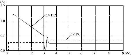
(4)Current fluctuation (Typ.) when power is turned on
Note:
Maximum current is 1.5 A and is continuance is 1.5 seconds
Figure 1.1 Current fluctuation (Typ.) when power is turned on
(5)Power on/off sequence
The voltage detector circuit monitors +5 V and +12 V. The circuit does not allow a write signal if either voltage is abnormal. This prevents data from being destroyed and eliminates the need to be concerned with the power on/off sequence.
C141-E045-02EN |
1 - 7 |
1.4Environmental Specifications
Table 1.4 lists the environmental specifications.
|
Table 1.4 |
Environmental specifications |
|
|
|
|
|
Temperature |
|
|
|
• |
Operating |
|
5°C to 55°C (ambient) |
|
|
|
5°C to 60°C (disk enclosure surface) |
• |
Non-operating |
|
–40°C to 60°C |
• |
Thermal Gradient |
|
20°C/h or less |
|
|
|
|
Humidity |
|
|
|
• |
Operating |
|
8% to 80%RH (Non-condensing) |
• |
Non-operating |
|
5% to 85%RH (Non-condensing) |
• |
Maximum Wet Bulb |
|
29°C |
|
|
|
|
Altitude (relative to sea level) |
|
|
|
• |
Operating |
|
–60 to 3,000 m (–200 to 10,000 ft) |
• |
Non-operating |
|
–60 to 12,000 m (–200 to 40,000 ft) |
|
|
|
|
1.5Acoustic Noise
Table 1.5 lists the acoustic noise specification.
Table 1.5 Acoustic noise specification
|
Operating |
Model |
MPB3021AT |
MPB3032AT |
MPB3052AT |
|
|
|
|
MPB3043AT |
MPB3064AT |
||
|
mode |
|
|
|||
|
|
|
|
|
||
Sound Power |
Idle mode |
|
3.6 bels |
3.7 bels |
3.8 bels |
|
per ISO7779 and ISO9296 |
(DRIVE READY) |
|||||
|
|
|
||||
(Typical at 1m) |
|
|
|
|
|
|
Seek mode (Random) |
4.2 bels |
4.3 bels |
4.3 bels |
|||
|
||||||
|
|
|
|
|
|
|
Sound Pressure |
Idle mode |
|
|
35 dBA |
|
|
(Typical at 1m) |
(DRIVE READY) |
|
|
|||
|
|
|
||||
|
|
|
|
|
||
|
Seek mode (Random) |
|
40 dBA |
|
||
|
|
|
|
|
|
|
1 - 8 |
C141-E045-02EN |

1.6Shock and Vibration
Table 1.6 lists the shock and vibration specification.
|
Table 1.6 Shock and vibration specification |
||
|
|
|
|
Vibration (swept sine, one octave per minute) |
|
|
|
• |
Operating |
5 to 300 Hz, 0.5G-0-peak |
|
|
|
(without non-recovered errors) |
|
• |
Non-operating |
5 to 400 Hz, 4G-0-peak (no damage) |
|
|
|
|
|
Shock (half-sine pulse, 11 ms duration) |
|
|
|
• |
Operating |
10G |
(without non-recovered errors) |
• |
Non-operating |
75G |
(no damage) |
|
|
|
|
1.7Reliability
(1)Mean time between failures (MTBF)
The mean time between failures (MTBF) is 500,000 H or more (operation: 24 hours/day, 7 days/week).
This does not include failures occurring during the first three months after installation. MTBF is defined as follows:
Total operation time in all fields
MTBF= number of device failure in all fields (H)
"Disk drive defects" refers to defects that involve repair, readjustment, or replacement. Disk drive defects do not include failures caused by external factors, such as damage caused by handling, inappropriate operating environments, defects in the power supply host system, or interface cable.
(2)Mean time to repair (MTTR)
The mean time to repair (MTTR) is 30 minutes or less, if repaired by a specialist maintenance staff member.
(3)Service life
In situations where management and handling are correct, the disk drive requires no overhaul for five years when the DE surface temperature is less than 48°C. When the DE surface temperature exceeds 48°C, the disk drives requires no overhaul for five years or 20,000 hours of operation, whichever occurs first. Refer to item (3) in Subsection 3.2 for the measurement point of the DE surface temperature.
C141-E045-02EN |
1 - 9 |
(4)Data assurance in the event of power failure
Except for the data block being written to, the data on the disk media is assured in the event of any power supply abnormalities. This does not include power supply abnormalities during disk media initialization (formatting) or processing of defects (alternative block assignment).
1.8Error Rate
Known defects, for which alternative blocks can be assigned, are not included in the error rate count below. It is assumed that the data blocks to be accessed are evenly distributed on the disk media.
(1)Unrecoverable read error
Read errors that cannot be recovered by maximum 126 times read retries without user's retry and ECC corrections shall occur no more than 10 times when reading data of 1015 bits. Read retries are executed according to the disk drive's error recovery procedure, and include read retries accompanying head offset operations.
(2)Positioning error
Positioning (seek) errors that can be recovered by one retry shall occur no more than 10 times in 107 seek operations.
1.9Media Defects
Defective sectors are replaced with alternates when the disk is formatted prior to shipment from the factory (low level format). Thus, the host sees a defect-free device.
Alternate sectors are automatically accessed by the disk drive. The user need not be concerned with access to alternate sectors.
Chapter 6 describes the low level format at shipping.
1 - 10 |
C141-E045-02EN |

CHAPTER 2 DEVICE CONFIGURATION
2.1Device Configuration
2.2System Configuration
2.1Device Configuration
Figure 2.1 shows the disk drive. The disk drive consists of a disk enclosure (DE), read/write preamplifier, and controller PCA. The disk enclosure contains the disk media, heads, spindle motors actuators, and a circulating air filter.
Figure 2.1 Disk drive outerview
C141-E045-02EN |
2 - 1 |
(1)Disk
The outer diameter of the disk is 95 mm. The inner diameter is 25 mm. The number of disks used varies with the model, as described below. The disks are rated at over 40,000 start/stop operations.
MPB3021AT: 1 disk MPB3032AT: 2 disks MPB3043AT: 2 disks MPB3052AT: 3 disks MPB3064AT: 3 disks
(2)Head
The heads are of the contact start/stop (CSS) type. The head touches the disk surface while the disk is not rotating and automatically lifts when the disk starts.
Figure 2.2 illustrates the configuration of the disks and heads of each model. In the disk surface, servo information necessary for controlling positioning and read/write and user data are written. Numerals 0 to 5 indicate read/write heads.
2 - 2 |
C141-E045-02EN |
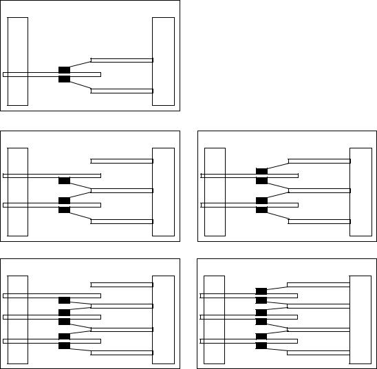
MPB3021ATModelModel
Spindle |
Actuator |
1 |
|
0 |
|
MPB3032ATT Model |
|
Spindle |
Actuator |
2 |
|
1 |
|
0 |
|
MPB3052AT Model |
|
Spindle |
Actuator |
4 |
|
3 |
|
2 |
|
1 |
|
0 |
|
MPB3043AT Model |
|
Spindle |
Actuator |
3 |
|
2 |
|
1 |
|
0 |
|
MPB3064AT Model |
|
Spindle |
Actuator |
5 |
|
4 |
|
3 |
|
2 |
|
1 |
|
0 |
|
Figure 2.2 Configuration of disk media heads
(3)Spindle motor
The disks are rotated by a direct drive Hall-less DC motor.
(4)Actuator
The actuator uses a revolving voice coil motor (VCM) structure which consumes low power and generates very little heat. The head assembly at the edge of the actuator arm is controlled and positioned by feedback of the servo information read by the read/write head. If the power is not on or if the spindle motor is stopped, the head assembly stays in the specific CSS zone on the disk and is fixed by a mechanical lock.
C141-E045-02EN |
2 - 3 |
(5)Air circulation system
The disk enclosure (DE) is sealed to prevent dust and dirt from entering. The disk enclosure features a closed loop air circulation system that relies on the blower effect of the rotating disk. This system continuously circulates the air through the circulation filter to maintain the cleanliness of the air within the disk enclosure.
(6)Read/write circuit
The read/write circuit uses a LSI chip for the read/write preamplifier. It improves data reliability by preventing errors caused by external noise.
(7)Controller circuit
The controller circuit consists of an LSI chip to improve reliability. The high-speed microprocessor unit (MPU) achieves a high-performance AT controller.
2.2System Configuration
2.2.1ATA interface
Figures 2.3 and 2.4 show the ATA interface system configuration. The drive has a 40-pin PC AT interface connector and supports the PIO transfer till 16.7 MB/s (ATA-3, Mode 4), the DMA transfer till 16.7 MB/s (ATA-3, Multiword mode 2), and the ultra DMA transfer till 33.3 MB/s (ATA-4, Ultra DMA mode 2).
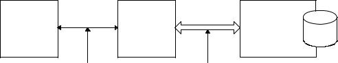
2.2.21 drive connection
Host |
HA |
Disk drive |
|
(Host adaptor) |
|||
|
|
||
AT bus |
|
ATA interface |
|
(Host interface) |
|
|
Figure 2.3 1 drive system configuration
2 - 4 |
C141-E045-02EN |
2.2.32 drives connection
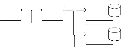
Host |
HA |
Disk drive #0 |
|
(Host adaptor) |
|||
|
|
AT bus (Host interface)
Disk drive #1
ATA interface
Note:
When the drive that is not conformed to ATA is connected to the disk drive is above configuration, the operation is not guaranteed.
Figure 2.4 2 drives configuration
IMPORTANT
HA (host adapter) consists of address decoder, driver, and receiver. ATA is an abbreviation of "AT attachment". The disk drive is conformed to the ATA-3 interface.
At high speed data transfer (PIO mode 3, mode 4, DMA mode 2 or ultra DMA mode 2), occurrence of ringing or crosstalk of the signal lines (AT bus) between the HA and the disk drive may be a great cause of the obstruction of system reliability. Thus, it is necessary that the capacitance of the signal lines including the HA and cable does not exceed the ATA-3 and ATA-4 standard, and the cable length between the HA and the disk drive should be as short as possible.
C141-E045-02EN |
2 - 5 |
Loading...