


 Loading...
C141-E261-01EN
MHW2120BK, MHW2080BK, MHW2060BK
DISK DRIVES
PRODUCT/MAINTENANCE MANUAL

FOR SAFE OPERATION
Handling of This Manual
This manual contains important information for using this product. Read thoroughly before using the product. Use this product only after thoroughly reading and understanding especially the section “Important Alert Items” in this manual. Keep this manual handy, and keep it carefully.
FUJITSU makes every effort to prevent users and bystanders from being injured or from suffering damage to their property. Use the product according to this manual.
IMPORTANT NOTE TO USERS
READ THE ENTIRE MANUAL CAREFULLY BEFORE USING THIS PRODUCT. INCORRECT USE OF THE PRODUCT MAY RESULT IN INJURY OR DAMAGE TO USERS, BYSTANDERS OR PROPERTY.
While FUJITSU has sought to ensure the accuracy of all information in this manual, FUJITSU assumes no liability to any party for any damage caused by any error or omission contained in this manual, its updates or supplements, whether such errors or omissions result from negligence, accident, or any other cause. In addition, FUJITSU assumes no liability with respect to the application or use of any product or system in accordance with the descriptions or instructions contained herein; including any liability for incidental or consequential damages arising therefrom. FUJITSU DISCLAIMS ALL WARRANTIES REGARDING THE INFORMATION CONTAINED HEREIN, WHETHER EXPRESSED, IMPLIED, OR STATUTORY.
FUJITSU reserves the right to make changes to any products described herein without further notice and without obligation.
This product is designed and manufactured for use in standard applications such as office work, personal devices and household appliances. This product is not intended for special uses (atomic controls, aeronautic or space systems, mass transport vehicle operating controls, medical devices for life support, or weapons firing controls) where particularly high reliability requirements exist, where the pertinent levels of safety are not guaranteed, or where a failure or operational error could threaten a life or cause a physical injury (hereafter referred to as "mission-critical" use). Customers considering the use of these products for mission-critical applications must have safety-assurance measures in place beforehand. Moreover, they are requested to consult our sales representative before embarking on such specialized use.
The contents of this manual may be revised without prior notice.
The contents of this manual shall not be disclosed in any way or reproduced in any media without the express written permission of Fujitsu Limited.
All Rights Reserved, Copyright FUJITSU LIMITED 2007
Revision History
(1/1)
Edition |
Date |
Revised section (*1) |
Details |
|
(Added/Deleted/Altered) |
||||
|
|
|
||
|
|
|
|
|
01 |
2007-05-31 |
|
|
|
|
|
|
|
|
|
|
|
|
*1 Section(s) with asterisk (*) refer to the previous edition when those were deleted.
C141-E261
This page is intentionally left blank.

Preface
This manual describes MHW2120BK, MHW2080BK, MHW2060BK model of the MHW Series, 2.5-inch hard disk drives. These drives have a built-in controller that is compatible with the Serial-ATA interface.
This manual describes the specifications and functions of the drives and explains in detail how to incorporate the drives into user systems. This manual assumes that the reader has a basic knowledge of hard disk drives and their implementations in computer systems.
This manual consists of seven chapters and sections explaining the special terminology and abbreviations used in this manual:
Overview of Manual
CHAPTER 1 Device Overview
This chapter gives an overview of the disk drive and describes their features.
CHAPTER 2 Device Configuration
This chapter describes the internal configurations of the disk drive and the configuration of the systems in which they operate.
CHAPTER 3 Installation Conditions
This chapter describes the external dimensions, installation conditions, and switch settings of the disk drive.
CHAPTER 4 Theory of Device Operation
This chapter describes the operation theory of the disk drive.
CHAPTER 5 Interface
This chapter describes the interface specifications of the disk drive.
CHAPTER 6 Operations
This chapter describes the operations of the disk drive.
CHAPTER 7 Maintenance and Diagnosis
This chapter explains the maintenance requirements, operation verification, troubleshooting, and removal/replacement of the disk drives.
Glossary
The glossary describes the technical terms that need to be understood to read this manual.
C141-E261 |
i |

Preface
Acronyms and Abbreviations
This section gives the meanings of the definitions used in this manual.
Conventions for Alert Messages
This manual uses the following conventions to show the alert messages. An alert message consists of an alert signal and alert statements. The alert signal consists of an alert symbol and a signal word or just a signal word.
The following are the alert signals and their meanings:
This indicates a hazardous situation could result in minor or moderate personal injury if the user does not perform the procedure correctly. This alert signal also indicates that damages to the product or other property may occur if the user does not perform the procedure correctly.
This indicates information that could help the user use the product more efficiently.
In the text, the alert signal is centered, followed below by the indented message. A wider line space precedes and follows the alert message to show where the alert message begins and ends. The following is an example:
(Example)
Data corruption: Avoid mounting the disk drive near strong magnetic sources such as loud speakers. Ensure that the disk drive is not affected by external magnetic fields.
The main alert messages in the text are also listed in the "Important Alert Items."
Operating Environment
This product is designed for mobile system as notebook PCs, and to be used within environmental specification. (please refer to the Chapter 1 in this manual.)
ii |
C141-E261 |

Preface
Conventions
An MHW series device is sometimes simply referred to as a "hard disk drive," "HDD," "drive," or "device" in this document.
Decimal numbers are represented normally.
Hexadecimal numbers are represented as shown in the following examples: X'17B9', 17B9h, 17B9H, or 17B9H.
Binary numbers are represented as shown in the following examples: 010 or 010b.
Serial-ATA may be referred to as "SATA".
Representation of the data storage capacity
One gigabyte (GB) = one billion bytes; accessible capacity will be less and actual capacity depends on the operating environment and formatting.
Attention
Please forward any comments you may have regarding this manual.
To make this manual easier for users to understand, opinions from readers are needed. Please write your opinions or requests on the Comment at the back of this manual and forward it to the address described in the sheet.
Liability Exception
"Disk drive defects" refers to defects that involve adjustment, repair, or replacement.
Fujitsu is not liable for any other disk drive defects, such as those caused by user misoperation or mishandling, inappropriate operating environments, defects in the power supply or cable, problems of the host system, or other causes outside the disk drive.
C141-E261 |
iii |

Preface
Hot Plug
These drives support Hot Plug which is based on Serial ATA Revision 2.5
Specification.
However, the disk drive installation and removal notes on safety precautions with regard to hot-plugging vary depending on the specific requirements and environment-related conditions of the system to which the drive is connected by hot-plugging.
When using the drive under general conditions of use (i.e., without hot-plugging), observe the important alert messages and notes on safety precautions given in this manual.
For the electrical recommendation to the host system which supports hot-plugging with this drives, refer to Section 5.1.6.
Compliance with Administration on the Control of Pollution Caused by Electronic Information Products of the People's Republic of China
This product is shipped as a component to manufacture the final products. Therefore, the packaging material code provided in GB18455-2001 is not marked on any packaging part of this product.
iv |
C141-E261 |

Important Alert Items
Important Alert Messages
The important alert messages in this manual are as follows:
A hazardous situation could result in minor or moderate personal injury if the user does not perform the procedure correctly. Also, damage to the product or other property, may occur if the user does not perform the procedure correctly.
Task |
Alert message |
Page |
|
|
|
Normal Operation |
Data corruption: Avoid mounting the disk near strong |
3-7 |
|
magnetic sources such as loud speakers. Ensure that the disk |
|
|
drive is not affected by external magnetic fields. |
|
|
Damage: Do not press the cover of the disk drive. Pressing |
|
|
it too hard, the cover and the spindle motor contact, which |
|
|
may cause damage to the disk drive. |
|
|
Static: When handling the device, disconnect the body |
|
|
ground (500 kΩ or greater). Do not touch the printed circuit |
|
|
board, but hold it by the edges. |
|
|
|
|
Maintenance |
Static, Damage |
|
|
1. Don’t install or remove a PCA or connect or disconnect |
7-2 |
|
a cable or connector plug when the drive is powered. |
|
|
This may give you an electric shock. |
|
|
2. Keep away from mechanical assemblies in the unit |
|
|
during operation. This may cause injuries. |
|
|
3. Avoid dangerous detergent when the disk drive is |
|
|
cleaned. |
|
|
|
|
C141-E261 |
v |

Important Alert Items
Task |
|
Alert message |
Page |
|
|
|
|
Maintenance |
Device damage |
|
|
|
1. |
Before touching a PCA or the drive, wear a wrist strap |
7-2 |
|
|
and perform the human body grounding to discharge |
|
|
|
static electricity from your body. This will prevent |
|
|
|
irreparable damage to the PCA and the head of the drive. |
|
|
2. |
Don’t install or remove a PCA or connect or disconnect |
|
|
|
a cable or connector plug when the drive is powered. |
|
|
|
This will prevent electrical damage to the disk drive. |
|
|
3. |
Operating the disk drive with one or more PCA missing |
|
|
|
will be unpredictable. Only power the drive with all |
|
|
|
boards installed. |
|
|
4. |
Avoid any detergent which may cause short circuits |
|
|
|
when cleaning assemblies. |
|
|
5. |
Keep all vents open opened and unblocked. Avoid other |
|
|
|
conditions which may cause circuits to overheat. |
|
|
6. |
Do not apply excessive force to the cover under any |
|
|
|
circumstances. Doing so may cause irreparable damage |
|
|
|
to the cover. |
|
|
Device damage |
|
|
|
The DE is completely sealed. Do not open the DE in the |
7-3 |
|
|
field. |
|
|
|
Data corruption |
|
|
|
When asking for repair, save all data stored in the disk drive |
7-4 |
|
|
beforehand. Fujitsu Limited is not responsible for any loss of |
|
|
|
data during service and repair. |
|
|
|
Device damage |
|
|
|
The disk enclosure (DE) must never to be opened in the field. |
7-14 |
|
|
Opening the disk enclosure may cause irreparable damage. |
|
|
|
Damage or Device damage |
|
|
|
1. |
Perform any removal after the system power is |
7-15 |
|
|
completely disconnected. The cable must not be |
|
|
|
disconnected and the screws that attach the drive must |
|
|
|
not be removed with the power ON. |
|
|
2. |
Do not move the drive and attach or detach the connector |
|
|
|
until it comes to a complete stop (about 30 s after the |
|
|
|
power is turned OFF). |
|
|
3. |
Perform the human body grounding to discharge any |
|
|
|
static electricity from your body. (Be sure to wear a |
|
|
|
wrist strap) |
|
|
|
|
|
vi |
C141-E261 |
Manual Organization
MHW2120BK, MHW2080BK |
|
• Device Overview |
MHW2060BK |
|
• Device Configuration |
|
|
• Installation Conditions |
DISK DRIVES |
|
• Theory of Device Operation |
PRODUCT/MAINTENANCE |
|
• Interface |
MANUAL |
|
• Operations |
(C141-E261) |
|
• Maintenance and Diagnosis |
<This manual> |
|
|
|
|
|
C141-E261 |
vii |
This page is intentionally left blank.

Contents
CHAPTER 1 |
Device Overview ....................................................................... |
1-1 |
|
1.1 |
Features .............................................................................................................. |
1-2 |
|
|
1.1.1 |
Functions and performance ..................................................................... |
1-2 |
|
1.1.2 |
Adaptability............................................................................................. |
1-2 |
|
1.1.3 |
Interface................................................................................................... |
1-3 |
1.2 |
Device Specifications......................................................................................... |
1-4 |
|
|
1.2.1 |
Specifications summary .......................................................................... |
1-4 |
|
1.2.2 Model and product number ..................................................................... |
1-5 |
|
1.3 |
Power Requirements .......................................................................................... |
1-6 |
|
1.4 |
Environmental Specifications ............................................................................ |
1-9 |
|
1.5 |
Acoustic Noise ................................................................................................. |
1-10 |
|
1.6 |
Shock and Vibration......................................................................................... |
1-10 |
|
1.7 |
Reliability......................................................................................................... |
1-11 |
|
1.8 |
Error Rate ......................................................................................................... |
1-12 |
|
1.9 |
Media Defects .................................................................................................. |
1-12 |
|
1.10 Load/Unload Function.................................................................................... |
1-12 |
||
|
1.10.1 Recommended power-off sequence .................................................... |
1-13 |
|
1.11 Advanced Power Management (APM) .......................................................... |
1-13 |
||
1.12 Interface Power Management (IPM).............................................................. |
1-15 |
||
|
1.12.1 |
Host-initiated interface power management (HIPM) .......................... |
1-15 |
|
1.12.2 |
Device-initiated interface power management (DIPM) ...................... |
1-15 |
CHAPTER 2 |
Device Configuration................................................................ |
2-1 |
|
2.1 |
Device Configuration ......................................................................................... |
2-2 |
|
C141-E261 |
ix |

Contents
2.2 |
System Configuration......................................................................................... |
2-3 |
|
|
2.2.1 |
SATA interface........................................................................................ |
2-3 |
|
2.2.2 |
Drive connection ..................................................................................... |
2-3 |
CHAPTER 3 |
Installation Conditions.............................................................. |
3-1 |
|
3.1 |
Dimensions......................................................................................................... |
3-2 |
|
3.2 |
Mounting ............................................................................................................ |
3-3 |
|
3.3 |
Connections with Host System........................................................................... |
3-9 |
|
|
3.3.1 |
Device connector ..................................................................................... |
3-9 |
|
3.3.2 |
Signal segment and power supply segment........................................... |
3-10 |
|
3.3.3 |
Connector specifications for host system .............................................. |
3-10 |
|
3.3.4 |
SATA interface cable connection.......................................................... |
3-11 |
|
3.3.5 |
Note about SATA interface cable connection ....................................... |
3-11 |
CHAPTER 4 |
Theory of Device Operation...................................................... |
4-1 |
|
4.1 |
Outline ................................................................................................................ |
4-2 |
|
4.2 |
Subassemblies..................................................................................................... |
4-2 |
|
|
4.2.1 |
Disk ......................................................................................................... |
4-2 |
|
4.2.2 |
Spindle..................................................................................................... |
4-2 |
|
4.2.3 |
Actuator ................................................................................................... |
4-2 |
|
4.2.4 |
Air filter................................................................................................... |
4-3 |
4.3 |
Circuit Configuration.......................................................................................... |
4-3 |
|
4.4 |
Power-on Sequence ............................................................................................ |
4-6 |
|
4.5 |
Self-calibration ................................................................................................... |
4-8 |
|
|
4.5.1 |
Self-calibration contents.......................................................................... |
4-8 |
|
4.5.2 |
Execution timing of self-calibration ........................................................ |
4-9 |
|
4.5.3 |
Command processing during self-calibration.......................................... |
4-9 |
4.6 |
Read/write Circuit ............................................................................................ |
4-10 |
|
|
4.6.1 |
Read/write preamplifier (PreAMP) ....................................................... |
4-10 |
|
4.6.2 |
Write circuit........................................................................................... |
4-10 |
x |
C141-E261 |

|
|
|
|
Contents |
|
|
|
|
|
|
4.6.3 |
Read circuit ........................................................................................... |
4-11 |
|
|
4.6.4 |
Digital PLL circuit ................................................................................ |
4-12 |
|
4.7 |
Servo Control ................................................................................................... |
4-13 |
||
|
4.7.1 |
Servo control circuit .............................................................................. |
4-13 |
|
|
4.7.2 |
Data-surface servo format ..................................................................... |
4-15 |
|
|
4.7.3 |
Servo frame format................................................................................ |
4-17 |
|
|
4.7.4 |
Actuator motor control .......................................................................... |
4-18 |
|
|
4.7.5 |
Spindle motor control............................................................................ |
4-19 |
|
CHAPTER 5 |
Interface..................................................................................... |
5-1 |
||
5.1 |
Physical Interface ............................................................................................... |
5-2 |
||
|
5.1.1 |
Interface signals....................................................................................... |
5-2 |
|
|
5.1.2 |
Signal interface regulation ...................................................................... |
5-4 |
|
|
5.1.3 |
Electrical specifications........................................................................... |
5-6 |
|
|
5.1.4 |
Connector pinouts ................................................................................... |
5-7 |
|
|
5.1.5 |
P11 function ............................................................................................ |
5-8 |
|
|
5.1.6 |
Hot Plug ................................................................................................ |
5-10 |
|
5.2 |
Logical Interface .............................................................................................. |
5-11 |
||
|
5.2.1 |
Communication layers........................................................................... |
5-12 |
|
|
5.2.2 |
Outline of the Shadow Block Register .................................................. |
5-13 |
|
|
5.2.3 |
Outline of the frame information structure (FIS) .................................. |
5-14 |
|
|
5.2.4 |
Shadow block registers.......................................................................... |
5-22 |
|
5.3 Host Commands ............................................................................................... |
5-27 |
|||
|
5.3.1 Command code and parameters ............................................................ |
5-27 |
||
|
5.3.2 Command descriptions.......................................................................... |
5-30 |
||
|
|
(1) |
RECALIBRATE (X '10' to X '1F')................................................ |
5-31 |
|
|
(2) |
READ SECTOR(S) (X '20' or X '21') ........................................... |
5-32 |
|
|
(3) |
WRITE SECTOR(S) (X '30' or X '31') ......................................... |
5-34 |
|
|
(4) |
WRITE VERIFY (X '3C') ............................................................. |
5-36 |
|
|
(5) |
READ VERIFY SECTOR(S) (X '40' or X '41')............................ |
5-38 |
|
|
(6) |
SEEK (X '70' to X '7F') ................................................................. |
5-40 |
|
|
(7) |
EXECUTE DEVICE DIAGNOSTIC (X '90')............................... |
5-41 |
|
|
(8) |
INITIALIZE DEVICE PARAMETERS (X '91') .......................... |
5-42 |
C141-E261 |
xi |

Contents
(9) |
DOWNLOAD MICROCODE (X '92').......................................... |
5-43 |
(10) |
STANDBY IMMEDIATE (X '94' or X 'E0') ................................ |
5-46 |
(11) |
IDLE IMMEDIATE (X '95' or X 'E1')/UNLOAD |
|
|
IMMEDIATE (X '95' or X 'E1') .................................................... |
5-47 |
(12) |
STANDBY (X '96' or X 'E2') ........................................................ |
5-49 |
(13) |
IDLE (X '97' or X 'E3') .................................................................. |
5-50 |
(14) |
CHECK POWER MODE (X '98' or X 'E5').................................. |
5-52 |
(15) |
SLEEP (X '99' or X 'E6') .............................................................. |
5-53 |
(16) |
SMART (X 'B0')............................................................................ |
5-54 |
(17) |
DEVICE CONFIGURATION (X 'B1') ......................................... |
5-84 |
(18) |
READ MULTIPLE (X 'C4').......................................................... |
5-89 |
(19) |
WRITE MULTIPLE (X 'C5') ........................................................ |
5-92 |
(20) |
SET MULTIPLE MODE (X 'C6')................................................. |
5-94 |
(21) |
READ DMA (X 'C8' or X 'C9') ..................................................... |
5-96 |
(22) |
WRITE DMA (X 'CA' or X 'CB').................................................. |
5-98 |
(23) |
READ BUFFER (X 'E4')............................................................. |
5-100 |
(24) |
FLUSH CACHE (X 'E7')............................................................. |
5-101 |
(25) |
WRITE BUFFER (X 'E8') ........................................................... |
5-102 |
(26) |
IDENTIFY DEVICE (X 'EC') ..................................................... |
5-103 |
(27) |
IDENTIFY DEVICE DMA (X 'EE') ........................................... |
5-104 |
(28) |
SET FEATURES (X 'EF') ........................................................... |
5-119 |
(29) |
SECURITY SET PASSWORD (X 'F1')...................................... |
5-126 |
(30) |
SECURITY UNLOCK (X 'F2')................................................... |
5-128 |
(31) |
SECURITY ERASE PREPARE (X 'F3') .................................... |
5-130 |
(32) |
SECURITY ERASE UNIT (X 'F4') ............................................ |
5-131 |
(33) |
SECURITY FREEZE LOCK (X 'F5') ......................................... |
5-132 |
(34) |
SECURITY DISABLE PASSWORD (X 'F6')............................ |
5-134 |
(35) |
READ NATIVE MAX ADDRESS (X 'F8')................................ |
5-136 |
(36) |
SET MAX (X 'F9')....................................................................... |
5-137 |
(37) |
READ SECTOR (S) EXT (X '24') .............................................. |
5-143 |
(38) |
READ DMA EXT (X '25') .......................................................... |
5-144 |
(39) |
READ NATIVE MAX ADDRESS EXT (X '27') ....................... |
5-145 |
(40) |
READ MULTIPLE EXT (X '29')................................................ |
5-146 |
(41) |
READ LOG EXT (X '2F') ........................................................... |
5-147 |
(42) |
WRITE SECTOR (S) EXT (X '34')............................................. |
5-153 |
(43) |
WRITE DMA EXT (X '35') ........................................................ |
5-154 |
xii |
C141-E261 |

|
|
|
Contents |
|
|
|
|
|
(44) |
SET MAX ADDRESS EXT (X '37')........................................... |
5-155 |
|
(45) |
WRITE MULTIPLE EXT (X '39').............................................. |
5-157 |
|
(46) |
WRITE DMA FUA EXT (X '3D') .............................................. |
5-158 |
|
(47) |
WRITE LOG EXT (X '3F') ......................................................... |
5-159 |
|
(48) |
READ VERIFY SECTOR (S) EXT (X '42')............................... |
5-163 |
|
(49) |
WRITE UNCORRECTABLE EXT (X '39') ............................... |
5-164 |
|
(50) |
READ LOG DMA EXT (X '47')................................................. |
5-166 |
|
(51) |
WRITE LOG DMA EX (X '57') ................................................. |
5-167 |
|
(52) |
READ FP DMA QUEUED (X '60')............................................ |
5-168 |
|
(53) |
WRITE FP DMA QUEUED (X '61') .......................................... |
5-169 |
|
(54) |
WRITE MULTIPLE FUA EXT (X 'CE').................................... |
5-170 |
|
(55) |
FLUSH CACHE EXT (X 'EA')................................................... |
5-171 |
|
5.3.3 Error posting........................................................................................ |
5-172 |
|
5.4 Command Protocol......................................................................................... |
5-174 |
||
|
5.4.1 Non-data command protocol............................................................... |
5-175 |
|
|
5.4.2 PIO data-in command protocol ........................................................... |
5-177 |
|
|
5.4.3 PIO data-out command protocol ......................................................... |
5-179 |
|
|
5.4.4 DMA data-in command protocol ........................................................ |
5-181 |
|
|
5.4.5 DMA data-out command protocol ...................................................... |
5-182 |
|
|
5.4.6 Native Command Queuing protocol.................................................... |
5-183 |
|
5.5 Power-on and COMRESET ........................................................................... |
5-186 |
||
CHAPTER 6 |
Operations................................................................................. |
6-1 |
|
6.1 |
Reset and Diagnosis ........................................................................................... |
6-2 |
|
|
6.1.1 Response to power-on ............................................................................. |
6-2 |
|
|
6.1.2 Response to COMRESET ....................................................................... |
6-4 |
|
|
6.1.3 Response to a software reset ................................................................... |
6-7 |
|
6.2 Power Save |
......................................................................................................... |
6-8 |
|
|
6.2.1 Power save mode..................................................................................... |
6-8 |
|
|
6.2.2 Power commands .................................................................................. |
6-10 |
|
C141-E261 |
xiii |

Contents
6.3 |
Power Save Controlled by Interface Power Management (IPM) ..................... |
6-11 |
|
|
6.3.1 |
Power save mode of the interface.......................................................... |
6-11 |
6.4 |
Read-ahead Cache ............................................................................................ |
6-13 |
|
|
6.4.1 |
Data buffer structure.............................................................................. |
6-13 |
|
6.4.2 |
Caching operation.................................................................................. |
6-14 |
|
6.4.3 |
Using the read segment buffer............................................................... |
6-16 |
6.5 |
Write Cache ...................................................................................................... |
6-20 |
|
|
6.5.1 |
Cache operation ..................................................................................... |
6-20 |
CHAPTER 7 |
Maintenance and Diagnosis ..................................................... |
7-1 |
|
7.1 |
Maintenance ....................................................................................................... |
7-2 |
|
|
7.1.1 |
Rules for maintenance ............................................................................. |
7-2 |
|
7.1.2 |
Maintenance requirements....................................................................... |
7-3 |
|
7.1.3 |
Maintenance levels .................................................................................. |
7-5 |
|
7.1.4 |
Disk drive revision number ..................................................................... |
7-6 |
|
7.1.5 |
Tools and test equipment......................................................................... |
7-8 |
|
7.1.6 |
Self-diagnostics ....................................................................................... |
7-8 |
|
7.1.7 |
Test .......................................................................................................... |
7-8 |
7.2 |
Operation Confirmation.................................................................................... |
7-11 |
|
|
7.2.1 |
Operation test......................................................................................... |
7-11 |
|
7.2.2 |
Diagnostic test ....................................................................................... |
7-11 |
7.3 |
Troubleshooting Procedure .............................................................................. |
7-12 |
|
|
7.3.1 |
Troubleshooting procedure.................................................................... |
7-12 |
|
7.3.2 |
Troubleshooting disk drive replaced in field......................................... |
7-12 |
|
7.3.3 |
Troubleshooting at factory .................................................................... |
7-14 |
7.4 |
Disk Drive Removal Procedure........................................................................ |
7-15 |
|
7.5 |
Spare Disk Drive .............................................................................................. |
7-15 |
|
xiv |
C141-E261 |

|
Contents |
|
|
Glossary............................................................................................................ |
GL-1 |
Acronyms and Abbreviations ........................................................................ |
AB-1 |
Index .................................................................................................................. |
IN-1 |
C141-E261 |
xv |

Contents
Illustrations
Figures
Figure 1.1 |
Permissible range of +5V rise slope ..................................................... |
1-6 |
Figure 1.2 The example of negative voltage waveform at +5 V |
|
|
|
when power is turned off...................................................................... |
1-7 |
Figure 1.3 |
Current fluctuation (Typ.) at +5 V when power is turned on ............... |
1-9 |
Figure 2.1 |
Disk drive outerview ............................................................................ |
2-2 |
Figure 2.2 |
Drive system configuration................................................................... |
2-3 |
Figure 3.1 |
Dimensions ........................................................................................... |
3-2 |
Figure 3.2 |
Mounting frame structure ..................................................................... |
3-4 |
Figure 3.3 |
Location of breather.............................................................................. |
3-5 |
Figure 3.4 |
Surface cover temperature measurement points ................................... |
3-6 |
Figure 3.5 |
Service area........................................................................................... |
3-7 |
Figure 3.6 |
Handling cautions ................................................................................. |
3-8 |
Figure 3.7 |
Connector locations .............................................................................. |
3-9 |
Figure 3.8 Power supply pins (CN1) ................................................................... |
3-10 |
|
Figure 4.1 |
Power supply configuration.................................................................. |
4-4 |
Figure 4.2 |
Circuit configuration............................................................................. |
4-5 |
Figure 4.3 |
Power-on operation sequence............................................................... |
4-7 |
Figure 4.4 |
Read/write circuit block diagram........................................................ |
4-10 |
Figure 4.5 |
Frequency characteristic of programmable filter................................ |
4-11 |
Figure 4.6 |
Block diagram of servo control circuit ............................................... |
4-13 |
Figure 4.7 |
Physical sector servo configuration on disk surface........................... |
4-16 |
Figure 4.8 |
Servo frame format............................................................................. |
4-17 |
Figure 5.1 |
Interface signals.................................................................................... |
5-2 |
Figure 5.2 |
Example of the circuit for driving Activity LED.................................. |
5-9 |
Figure 5.3 |
Conceptual diagram of communication layers ................................... |
5-11 |
Figure 5.4 |
Register - Host to Device FIS layout.................................................. |
5-15 |
Figure 5.5 |
Register - Device to Host FIS layout.................................................. |
5-16 |
Figure 5.6 DMA Active - Device to Host FIS layout .......................................... |
5-16 |
|
Figure 5.7 DMA Setup - Device to Host or Host to Device FIS layout............... |
5-17 |
|
Figure 5.8 |
BIST Active - Bidirectional FIS layout .............................................. |
5-18 |
Figure 5.9 |
Data FIS (Bidirectional) layout .......................................................... |
5-19 |
Figure 5.10 |
PIO Setup - Device to Host FIS layout............................................. |
5-19 |
xvi |
C141-E261 |
|
|
Contents |
|
|
|
Figure 5.11 |
Set Device Bits FIS .......................................................................... |
5-21 |
Figure 5.12 Execution example of READ MULTIPLE command...................... |
5-90 |
|
Figure 5.13 Non-data command protocol .......................................................... |
5-176 |
|
Figure 5.14 PIO data-in command protocol ...................................................... |
5-178 |
|
Figure 5.15 PIO data-out command protocol .................................................... |
5-180 |
|
Figure 5.16 DMA data-in command protocol.................................................... |
5-181 |
|
Figure 5.17 DMA data-out command protocol.................................................. |
5-182 |
|
Figure 5.18 READ FP DMA QUEUED command protocol ............................. |
5-184 |
|
Figure 5.19 WRITE FP DMA QUEUED command protocol ........................... |
5-185 |
|
Figure 5.20 Power-on sequence......................................................................... |
5-186 |
|
Figure 5.21 COMRESET sequence ................................................................... |
5-187 |
|
Figure 6.1 |
Response to power-on (when the host is powered on earlier |
|
|
than the device) .................................................................................... |
6-2 |
Figure 6.2 |
Response to power-on (when the device is powered on |
|
|
earlier than the host)............................................................................. |
6-3 |
Figure 6.3 Response to COMRESET .................................................................... |
6-4 |
|
Figure 6.4 |
Response to a software reset................................................................. |
6-7 |
Figure 6.5 |
Data buffer structure........................................................................... |
6-13 |
Figure 7.1 |
Disk drive revision number label ......................................................... |
7-6 |
Figure 7.2 |
Display of disk drive revision number ................................................. |
7-7 |
Figure 7.3 |
Test flowchart....................................................................................... |
7-9 |
C141-E261 |
xvii |

Contents
Tables
Table 1.1 |
Specifications ........................................................................................ |
1-4 |
Table 1.2 Examples of model names and product numbers................................... |
1-5 |
|
Table 1.3 |
Current and power dissipation ............................................................... |
1-8 |
Table 1.4 |
Environmental specifications................................................................. |
1-9 |
Table 1.5 |
Acoustic noise specification................................................................. |
1-10 |
Table 1.6 |
Shock and vibration specification ........................................................ |
1-10 |
Table 1.7 Advanced Power Management ............................................................ |
1-14 |
|
Table 1.8 Interface power management ............................................................... |
1-16 |
|
Table 3.1 |
Surface temperature measurement points and standard values.............. |
3-6 |
Table 5.1 |
Connector pinouts .................................................................................. |
5-7 |
Table 5.2 |
Requirements for P11 as an output pin. ................................................. |
5-9 |
Table 5.3 Shadow Block Register........................................................................ |
5-13 |
|
Table 5.4 BIST combinations .............................................................................. |
5-18 |
|
Table 5.5 Command code and parameters .......................................................... |
5-27 |
|
Table 5.6 |
Diagnostic code.................................................................................... |
5-41 |
Table 5.7 Operation of DOWNLOAD MICROCODE........................................ |
5-44 |
|
Table 5.8 |
Example of rewriting procedure of data 640K Bytes |
|
|
(A0000h Bytes) of microcode ........................................................... |
5-45 |
Table 5.9 |
Features Field values (subcommands) and functions .......................... |
5-55 |
Table 5.10 |
Format of device attribute value data................................................. |
5-59 |
Table 5.11 |
Format of guarantee failure threshold value data............................... |
5-59 |
Table 5.12 |
Off-line data collection status ............................................................ |
5-62 |
Table 5.13 |
Self-test execution status.................................................................... |
5-62 |
Table 5.14 |
Off-line data collection capability...................................................... |
5-63 |
Table 5.15 |
Failure prediction capability flag ....................................................... |
5-63 |
Table 5.16 |
Drive error logging capability............................................................ |
5-64 |
Table 5.17 Log Directory Data Format................................................................ |
5-64 |
|
Table 5.18 Data format of SMART Summary Error Log ................................... |
5-65 |
|
Table 5.19 Data format of SMART Comprehensive Error Log .......................... |
5-67 |
|
Table 5.20 |
SMART self-test log data format....................................................... |
5-68 |
Table 5.21 |
Selective self-test log data structure................................................... |
5-69 |
Table 5.22 |
Selective self-test feature flags........................................................... |
5-70 |
Table 5.23 SCT command and the function......................................................... |
5-71 |
|
Table 5.24 Format of SCT STATUS Response ................................................... |
5-73 |
|
Table 5.25 SCT STATUS code............................................................................ |
5-75 |
|
Table 5.26 |
Action code ........................................................................................ |
5-77 |
Table 5.27 WRITE SAME .................................................................................. |
5-77 |
|
xviii |
C141-E261 |

|
|
Contents |
|
|
|
Table 5.28 ERROR RECOVERY CONTROL.................................................... |
5-78 |
|
Table 5.29 FEATURE CONTROL COMMAND ............................................... |
5-79 |
|
Table 5.30 SCT DATA TABLE .......................................................................... |
5-80 |
|
Table 5.31 HAD Temperature ............................................................................. |
5-81 |
|
Table 5.32 DEVICE CONFIGURATION IDENTIFY data structure ................ |
5-87 |
|
Table 5.33 Information to be read by IDENTIFY DEVICE command............. |
5-105 |
|
Table 5.34 |
Features field values and settable modes ........................................ |
5-119 |
Table 5.35 Contents of SECURITY SET PASSWORD data............................ |
5-126 |
|
Table 5.36 |
Relationship between combination of Identifier and Security |
|
|
level, and operation of the lock function......................................... |
5-126 |
Table 5.37 |
Contents of security password ......................................................... |
5-134 |
Table 5.38 Data format of Read Log Ext log page 10h ..................................... |
5-149 |
|
Table 5.39 |
Tag field information....................................................................... |
5-149 |
Table 5.40 Data format of Read Log Ext log page 11h ..................................... |
5-150 |
|
Table 5.41 |
Counter Identifier information......................................................... |
5-150 |
Table 5.42 Operation mode ............................................................................... |
5-165 |
|
Table 5.43 Command code and parameters ...................................................... |
5-172 |
|
Table 7.1 |
Status Field contents ............................................................................ |
7-10 |
Table 7.2 |
Disposition for Error Field contents .................................................... |
7-10 |
Table 7.3 |
System level and field troubleshooting................................................ |
7-13 |
C141-E261 |
xix |
This page is intentionally left blank.

CHAPTER 1 Device Overview
1.1Features
1.2Device Specifications
1.3Power Requirements
1.4Environmental Specifications
1.5Acoustic Noise
1.6Shock and Vibration
1.7Reliability
1.8Error Rate
1.9Media Defects
1.10Load/Unload Function
1.11Advanced Power Management (APM)
1.12Interface Power Management (IPM)
Overview and features are described in this chapter, and specifications and power requirement are described.
The disk drive is 2.5-inch hard disk drives with built-in disk controllers. These disk drives use the SATA interface protocol which has a high-speed interface data transfer rate.
C141-E261 |
1-1 |

Device Overview
1.1 Features
1.1.1 Functions and performance
The following features of the disk drive are described.
(1) Compact
The disk drive has up to 2 disks of 65 mm (2.5 inches) diameter, and its height is
9.5mm (0.374 inch).
(2)Environmental Protection
The disk drive comply with the Restriction of the use of certain Hazardous Substances in electrical and electronic equipment (RoHS) directive issued by European Union (EU).
(3) Large capacity
The disk drive can record up to 80 GB (formatted) on one disk using the RLL recording method and 30 recording zone technology. The disk drive has a formatted capacity of 120 GB (MHW2120BK), 80 GB (MHW2080BK), and 60 GB (MHW2060BK) respectively.
(4) High-speed Transfer rate
The disk drive (the MHW2xxxBK Series) has an internal data rate up to
96.6 MB/s. The disk drive supports an external data rate 3.0 Gbps (300 MB/s) (Serial-ATA Generation-2). And the disk drive realizes a high performance by high-speed transfer rate combined with Native Command Queuing (NCQ).
(5) Average positioning time
Use of a rotary voice coil motor in the head positioning mechanism greatly increases the positioning speed. The average positioning time is 10.5 ms (at read).
1.1.2 Adaptability
(1) Power save mode
The disk drive is ideal for applications since it supports the power save mode function that works in each of the Idle, Standby, and Sleep modes and has the Partial and Slumber interface power management functions. And automatically power down by APM function makes the disk drive ideal for mobile use where power consumption is a factor.
(2) Operating temperature
The disk drive can be used within the temperature range (5 °C to 60 °C at DE surface). (For details of the reliability for each temperature range, refer to the Section 1.7, "Reliability".)
1-2 |
C141-E261 |

1.1 Features
(3) Low noise and vibration
In Ready status (while the device is waiting for any commands), the Sound Power level of the disk drives in idle mode is 2.0B [MHW2060BK] / 2.5B [MHW2080BK, MHW2120BK]. The Sound Pressure level is 23dB [MHW2060BK] / 29dB [MHW2080BK, MHW2120BK], as measured 0.3 m from the drive in Idle mode.
(4) High resistance against shock
The Load/Unload mechanism is highly resistant against non-operation shock up to 8820 m/s2 (900G).
(5) Improved resistance against rotational vibration
The disk drive has built-in functions designed to minimize the adverse effects of rotational vibration to prevent performance degradation. (Rotational vibration can occur when multiple drive mechanisms are mounted in a single chassis.)
1.1.3 Interface
(1) Connection to SATA interface
The disk drive has built-in controllers compatible with the SATA interface.
(2) Data buffer
The disk drive uses the data buffer to transfer data between the host and the disk media.
In combination with the read-ahead cache system described in item (3) and the write cache described in item (6), the buffer contributes to efficient I/O processing.
(3) Read-ahead cache system
After the execution of a disk read command, the disk drive automatically reads the subsequent data block and writes it to the data buffer (read ahead operation). This cache system enables fast data access. The next disk read command would normally cause another disk access. But, if the read ahead data corresponds to the data requested by the next read command, the data in the buffer can be transferred instead.
(4) Error correction and retry by ECC
If a recoverable error occurs, the disk drive itself attempts error recovery. The ECC has improved buffer error correction for correctable data errors.
(5) Self-diagnosis
The disk drive has a diagnostic function to check operation of the controller and disk drive. Executing a diagnostic function of the smart command invokes self-diagnosis.
C141-E261 |
1-3 |

Device Overview
(6) Write cache
When the disk drive receives a write command, the disk drive posts the command completion at completion of transferring data to the data buffer completion of writing to the disk media. This feature reduces the access time at writing.
1.2 Device Specifications
1.2.1 Specifications summary
Table 1.1 shows the specifications of the disk drives.
Table 1.1 Specifications (1/2)
|
|
MHW2120BK |
|
MHW2080BK |
|
MHW2060BK |
|
|
|
|
|
|
|
Format Capacity (*1, *2) |
120 GB |
|
80 GB |
|
60 GB |
|
|
|
|
|
|
|
|
Number of Sectors (User) |
234,441,648 |
|
156,301,488 |
|
117,210,240 |
|
|
|
|
|
|
|
|
Bytes per Sector |
|
|
512 bytes |
|
||
|
|
|
|
|
||
Rotational Speed |
|
|
7,200 rpm ± 1% |
|
||
|
|
|
|
|
||
Average Latency |
|
|
4.17 ms |
|
||
|
|
|
|
|
|
|
Positioning time (read and seek) |
|
|
|
|
|
|
• |
Minimum (Track-Track) |
|
|
1.5 ms (typ.) |
|
|
• |
Average |
|
|
Read: 10.5 ms (typ.) |
|
|
• |
Maximum (Full) |
|
|
20.5 ms (typ.) |
|
|
|
|
|
|
|
||
Start time |
|
|
4.0 sec (typ.) |
|
||
|
|
|||||
Interface |
Compliant with ATA-8 ACS AST, Serial ATA Revision 2.5 |
|||||
|
|
|
|
Gen1i and Gen2i |
|
|
|
|
|
|
|
|
|
Data Transfer Rate (*3) |
|
|
|
|
|
|
• |
To/From Media |
|
|
96.6 MB/s Max. |
|
|
• |
To/From Host |
1.5 Gbps (150 MB/s) (Gen1i) |
||||
|
|
3.0 Gbps (300 MB/s) (Gen2i) |
||||
|
|
|
|
|||
Data Buffer Size (*4) |
|
8 MB (8,388,608 bytes) |
|
|||
|
|
|||||
Physical Dimensions |
9.5 mm × 100.0 mm × 70.0 mm (*5) |
|||||
(Height × Width × Depth) |
|
|
|
|
|
|
|
|
|
|
|
||
Weight |
|
|
116 g (Max.) |
|
||
|
|
|
|
|
|
|
*1: Capacity under the LBA mode.
*2: One gigabyte (GB) = one billion bytes and One megabyte (MB) = one million bytes; accessible capacity will be less and actual capacity depends on the operating environment and formatting.
*3: 1 GB is equal to 1,000,000,000 bytes and 1 MB is equal to 1,000,000 bytes.
1-4 |
C141-E261 |

1.2 Device Specifications
*4: 1 MB is equal to 1,048,576 bytes; the actual buffer capacity for data transfer will be less. Refer to the Section 6.4 of this manual.
*5: The value of Depth (=100.0 mm) does not include PCBA (Printed Circuit Board Assembly). For details, see Section 3.1.
Table 1.1 lists the formatted capacity, number of logical cylinders, number of heads, and number of sectors of every model for which the CHS mode has been selected using the BIOS setup utility on the host.
Table 1.1 Specifications (2/2)
Model |
Capacity (*1) |
No. of Cylinder |
No. of Heads |
No. of Sectors |
|
|
|
|
|
MHW2120BK |
8.45 GB |
16,383 |
16 |
63 |
|
|
|
|
|
MHW2080BK |
8.45 GB |
16,383 |
16 |
63 |
|
|
|
|
|
MHW2060BK |
8.45 GB |
16,383 |
16 |
63 |
|
|
|
|
|
*1: One gigabyte (GB) = one billion bytes; accessible capacity will be less and actual capacity depends on the operating environment and formatting.
1.2.2 Model and product number
Table 1.2 lists the model names and product numbers of the disk drive.
The model name does not necessarily correspond to the product number as listed in Table 1.2 since some models have been customized and have specifications that are different from those for the standard model.
If a disk drive is ordered as a replacement drive, the product number must be the same as that of the drive being replaced.
Table 1.2 Examples of model names and product numbers
Model Name |
Capacity (*1) |
Mounting screw |
Order No. |
|
(user area) |
||||
|
|
|
||
|
|
|
|
|
MHW2120BK |
120 GB |
M3 Depth 3 |
CA06855-B712 (1.5 Gbps model) |
|
CA06855-B742 (3.0 Gbps model) (*2) |
||||
|
|
|
||
|
|
|
|
|
MHW2080BK |
80 GB |
M3 Depth 3 |
CA06855-B728 (1.5 Gbps model) |
|
CA06855-B758 (3.0 Gbps model) (*2) |
||||
|
|
|
||
|
|
|
|
|
MHW2060BK |
60 GB |
M3 Depth 3 |
CA06855-B706 (1.5 Gbps model) |
|
CA06855-B736 (3.0 Gbps model) (*2) |
||||
|
|
|
||
|
|
|
|
*1: One gigabyte (GB) = one billion bytes; accessible capacity will be less and actual capacity depends on the operating environment and formatting.
*2: Serial ATA Generation-1 (1.5 Gbps) is also supported.
C141-E261 |
1-5 |
Device Overview
1.3 Power Requirements
(1) Input Voltage
• + 5 V ± 5 %
•It is unnecessary for this drive to supply +3.3 V and +12 V power supplies.
(2) Ripple
|
+5 V |
|
|
Maximum |
100 mV (peak to peak) |
|
|
Frequency |
DC to 1 MHz |
|
|
(3) Slope of an input voltage at rise
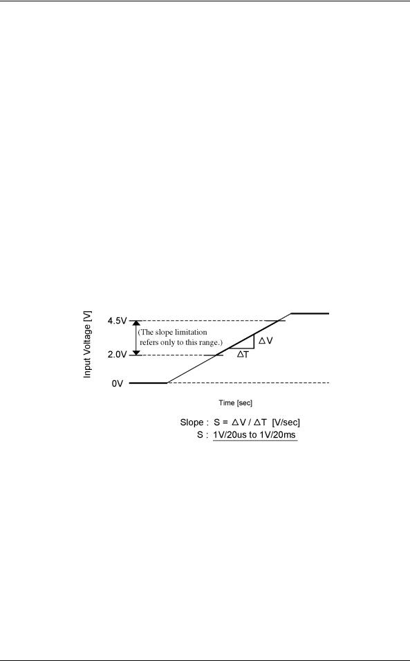
The following figure shows the restriction of the slope which is +5 V input voltage at rise. The permissible range of +5 V slope is from 1V/20 µsec to 1V/20 msec, under the voltage range is between 2.0V and 4.5V.
Figure 1.1 Permissible range of +5V rise slope
1-6 |
C141-E261 |
Loading...