


MQ372-02
Application Manual
Real Time Clock Module
RX-8581SA/JE/NB
Model |
Product Number |
RX-8581SA |
Q4185815xxxxx00 |
RX-8581JE |
Q4185817xxxxx00 |
RX-8581NB |
Q4185819xxxxx00 |

In pursuit of "Saving" Technology ,Epson electronic device.
Our Lineup of semiconductors, Liquid crystal displays and quartz devices assists in creating the products of our customers' dreams.
Epson IS energy savings.
NOTICE
•The material is subject to change without notice.
•Any part of this material may not be reproduced or duplicated in any form or any means without the written permission of Seiko Epson.
•The information, applied circuit, program, using way etc., written in this material is just for reference. Seiko Epson does not assume any liability for the occurrence of infringing any patent or copyright of third party. This material does not authorize the licence for any patent or intellectual property rights.
•Any product described in this material may contain technology or the subject relating to strategic products under the control of the Foreign Exchange and Foreign Trade Law of Japan and may require an export licence from the Ministry of International Trade and industry or other approval from another government agency.
•The products (except for some product for automotive applications) listed up on this material are designed to be used with ordinary electronic equipment (OA equipment, AV equipment, communications equipment, measuring instruments etc). Seiko Epson does not assume any liability for the case using the products with the appoication required high reliability or safety extremely (such as aerospace equipment etc).
When intending to use any our product with automotive application and the other application than ordinary electronic equipments as above, please contact our sales representatives in advance.

RX - 8581 SA / JE / NB
|
Contents |
|
1. |
Overview................................................................................................................... |
1 |
2. |
Block Diagram........................................................................................................ |
1 |
3. |
Terminal description............................................................................................. |
2 |
|
3.1. Terminal connections .............................................................................................................. |
2 |
|
3.2. Pin Functions ............................................................................................................................. |
2 |
4. |
Absolute Maximum Ratings .............................................................................. |
3 |
5. |
Recommended Operating Conditions ........................................................... |
3 |
6. |
Frequency Characteristics................................................................................. |
3 |
7. |
Electrical Characteristics.................................................................................... |
3 |
|
7.1. DC characteristics......................................................................................................................... |
3 |
|
7.2. AC Characteristics.................................................................................................................... |
4 |
8. |
Use Methods........................................................................................................... |
5 |
|
8.1. Overview of Functions............................................................................................................. |
5 |
|
8.2. Description of Registers ......................................................................................................... |
6 |
|
8.3. Fixed-cycle Timer Interrupt Function................................................................................ |
13 |
|
8.4. Time Update Interrupt Function ......................................................................................... |
16 |
|
8.5. Alarm Interrupt Function....................................................................................................... |
18 |
|
8.6. Reading/Writing Data via the I2C Bus Interface ........................................................... |
21 |
|
8.7. Backup and Recovery ........................................................................................................... |
25 |
|
8.8. Connection with Typical Microcontroller.......................................................................... |
25 |
9. |
External Dimensions / Marking Layout........................................................ |
26 |
10. Reference Data ................................................................................................. |
27 |
|
11. Application notes .............................................................................................. |
28 |
|
|
11.1. Notes on handling ................................................................................................................ |
28 |
|
11.2. Notes on packaging............................................................................................................. |
28 |

RX - 8581 SA / JE / NB
I2C-Bus Interface Real-time Clock Module
RX - 8581 SA / JE / NB
•Features built-in 32.768-kHz crystal oscillator, frequency adjusted
•Supports I2C-Bus's high speed mode (400 kHz)
•Alarm interrupt function for day, date, hour, and minute settings
•Fixed-cycle timer interrupt function
• Time update interrupt function |
(Seconds, minutes) |
|
• |
32.768-kHz output with OE function |
(FOE and FOUT pins) |
• |
Auto correction of leap years |
(from 2000 to 2099) |
•Wide interface voltage range: 1.8 V to 5.5 V
•Wide time-keeping voltage range:1.6 V to 5.5 V
•Low current consumption: 0.45 A /3 V (Typ.)
•Compact package (NB: SON− 22 pin PKG)
The I2C-Bus is a trademark of PHILIPS ELECTRONICS N.V.
1. Overview
This module is an I2C bus interface-compliant real-time clock which includes a 32.768-kHz crystal oscillator. In addition to providing a calendar (year, month, date, day, hour, minute, second) function and a clock counter function, this module provides an abundance of other functions including an alarm function, fixed-cycle timer function, time update interrupt function, and 32.768-kHz output function.
The devices in this module are fabricated via a C-MOS process for low current consumption, which enables long-term battery back-up.
All of these many functions are implemented in a thin, compact SON package, which makes it suitable for various kinds of mobile telephones and other small electronic devices.
2. Block Diagram
|
32.768 kHz |
|
|
|
DIVIDER |
CLOCK |
|
|
and |
||
|
OSC |
CALENDAR |
|
|
|
||
FOUT |
FOUT |
TIMER |
|
|
|||
FOE |
CONTROLLER |
REGISTER |
|
/ INT |
INTERRUPT |
ALARM |
|
CONTROLLER |
REGISTER |
||
|
|||
|
|
CONTROL |
|
SCL |
I2C-BUS |
REGISTER |
|
INTERFACE |
|
||
SDA |
and |
||
CIRCUIT |
|
||
|
SYSTEM |
||
|
|
||
|
|
CONTROLLER |
|
|
Page - 1 |
MQ372-02 |
RX - 8581 SA / JE / NB
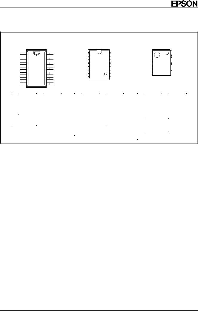
3. Terminal description
3.1. Terminal connections
RX - 8581 SA |
|
RX - 8581 JE |
|
RX - 8581 NB |
||||||
SOP − 14 pin |
|
VSOJ − 20 pin |
|
|
SON − 22 pin |
|||||
# 1 |
# 14 |
# 1 |
# 14 |
# 1 |
|
|
|
|
|
# 14 |
|
|
|
|
|
||||||
|
|
|||||||||
|
|
|||||||||
|
|
|
|
# 10 |
|
# 11 |
|
|
# 11 |
|
|
|
|
(#12) |
||
|
|
|
|
|
|
|
|
|
|
|
||||||
|
|
|
|
|
|
|
|
|
|
|
|
|
||||
# 7 |
|
|
# 8 |
|
|
|
|
|
|
|
|
|
|
|
|
|
|
|
|
|
|
|
|
|
|
|
|
|
|
|
|
|
|
No. |
Pin terminal |
No. |
Pin terminal |
|
No. |
Pin terminal |
No. |
Pin terminal |
|
No. |
Pin terminal |
No. |
Pin terminal |
|||
|
|
|
|
|
|
|
|
|
|
|
|
|
|
|
|
|
|
|
|
|
|
|
|
|
|
|
|
|
|
|
|
|
|
1 |
N.C. |
14 |
FOUT |
|
1 |
N.C. |
20 |
N.C. |
|
1 |
/ INT |
22 |
N.C. |
|||
2 |
SCL |
13 |
N.C. |
|
2 |
N.C. |
19 |
N.C. |
|
2 |
GND |
21 |
N.C. |
|||
3 |
SDA |
12 |
N.C. |
|
3 |
FOE |
18 |
N.C. |
|
3 |
( VDD ) |
20 |
N.C. |
|||
4 |
N.C. |
11 |
VDD |
|
4 |
VDD |
17 |
N.C. |
|
4 |
N.C. |
19 |
N.C. |
|||
5 |
GND |
10 |
FOE |
|
5 |
FOUT |
16 |
N.C. |
|
5 |
SDA |
18 |
N.C. |
|||
6 |
N.C. |
9 |
N.C. |
|
6 |
SCL |
15 |
N.C. |
|
6 |
SCL |
17 |
N.C. |
|||
7 |
/ INT |
8 |
N.C. |
|
7 |
SDAT |
14 |
N.C. |
|
7 |
FOUT |
16 |
N.C. |
|||
|
|
|
|
|
8 |
( VDD ) |
13 |
N.C. |
|
8 |
VDD |
15 |
N.C. |
|||
|
|
|
|
|
9 |
GND |
12 |
N.C. |
|
9 |
FOE |
14 |
N.C. |
|||
|
|
|
|
|
10 |
/ INT |
11 |
N.C. |
|
10 |
N.C. |
(13) |
− |
|||
|
|
|
|
|
|
|
|
|
|
11 |
N.C. |
(12) |
− |
|||
3.2. Pin Functions
Signal |
I/O |
Function |
|
name |
|||
|
|
||
|
|
|
|
SCL |
I |
This is the serial clock input pin for I2C Bus communications. |
|
|
|
|
|
|
|
This pin's signal is used for input and output of address, data, and ACK bits, |
|
SDA |
I/O |
synchronized with the serial clock used for I2C communications. |
|
Since the SDA pin is an N-ch open drain pin during output, be sure to connect a suitable |
|||
|
|
||
|
|
pull-up resistance relative to the signal line capacity. |
|
|
|
|
|
|
|
This is the C-MOS output pin with output control provided via the FOE pin. |
|
FOUT |
O |
When FOE = "H" (high level), this pin outputs a 32.768-kHz signal. |
|
|
|
When output is stopped, the FOUT pin = "L" (low level). |
|
|
|
|
|
|
|
This is an input pin used to control the output mode of the FOUT pin. |
|
FOE |
I |
When this pin's level is high, the FOUT pin is in output mode. When it is low, output via the |
|
|
|
FOUT pin is stopped. |
|
|
|
|
|
/INT |
O |
This pins is used to output alarm signals, timer signals, time update signals, and other |
|
signals. This pin is an open drain pin. |
|||
|
|
||
|
|
|
|
VDD |
− |
This pin is connected to a positive power supply. |
|
|
|
|
|
(VDD) |
− |
Although this pin has the same potential as VDD, it should not be connected externally. |
|
|
|
|
|
GND |
− |
This pin is connected to a ground. |
|
|
|
|
|
|
|
This pin is not connected to the internal IC. |
|
N.C. |
− |
Leave N.C. pins open or connect them to GND or VDD. |
|
(Note) Note with caution that in the RX-8581NB (SON-22 pin), the N.C. pins (pins 14 to |
|||
|
|
||
|
|
22) are interconnected via the internal frame. |
|
|
|
|
Note: Be sure to connect a bypass capacitor rated at least 0.1 µF between VDD and GND.
Page - 2 |
MQ372-02 |

RX - 8581 SA / JE / NB
4. Absolute Maximum Ratings
GND = 0 V
Item |
Symbol |
Condition |
Rating |
Unit |
|||
|
|
|
|
|
|
|
|
Supply voltage |
VDD |
Between VDD and GND |
− 0.3 |
to |
+7.0 |
V |
|
Input voltage (1) |
VIN1 |
FOE pin |
GND− 0.3 |
to |
VDD+0.3 |
V |
|
Input voltage (2) |
VIN2 |
SCL and SDA pins |
GND− 0.3 |
to |
+8.0 |
V |
|
Output voltage (1) |
VOUT1 |
FOUT pin |
GND− 0.3 |
to |
VDD+0.3 |
V |
|
Output voltage (2) |
VOUT2 |
SDA and /INT pins |
GND− 0.3 |
to |
+8.0 |
V |
|
Storage temperature |
TSTG |
When stored separately, |
− 55 |
to |
+125 |
° C |
|
without packaging |
|||||||
|
|
|
|
|
|
||
5. Recommended Operating Conditions |
|
|
|
|
|
|
GND = 0 V V |
|||||
Item |
Symbol |
Condition |
|
Min. |
|
Typ. |
Max. |
|
Unit |
|||
|
|
|
|
|
|
|
|
|
|
|
||
Operating supply voltage |
VDD |
− |
|
1.8 |
|
3.0 |
5.5 |
|
V |
|||
Clock supply voltage |
VCLK |
− |
|
1.6 |
|
3.0 |
5.5 |
|
V |
|||
Operating temperature |
TOPR |
No condensation |
|
|
− 40 |
|
+25 |
+85 |
|
° C |
||
6. Frequency Characteristics |
|
|
|
|
|
|
|
GND = 0 V |
||||
Item |
Symbol |
Condition |
|
|
Rating |
|
|
Unit |
||||
|
|
|
|
|
|
|
|
|
|
|
|
|
Frequency precision |
∆ f /f |
DD |
|
5 |
± |
23.0 |
( 1) |
|
× |
10 |
-6 |
|
|
Ta = +25 ° C, V = 3.0 V |
|
|
|
|
|
||||||
Frequency/voltage |
f /V |
Ta = +25 ° C, VDD = 2.0 V to 5.0 V |
|
± |
|
2 Max. |
|
× 10-6 /V |
||||
characteristics |
|
|
|
|
|
|
|
|
|
|
|
|
Frequency/temperature |
Top |
Ta = − 10 ° C to +70 ° C, |
|
+10 / − 120 |
|
× |
10− 6 |
|||||
characteristics |
VDD = 3.0 V ; +25 ° C reference |
|
|
|||||||||
|
|
|
|
|
|
|
|
|
|
|||
Oscillation start time |
tSTA |
Ta = +25 ° C, VDD = 3.0 V |
|
|
|
3 Max. |
|
|
s |
|
||
Aging |
fa |
Ta = +25 ° C, VDD = 3.0 V, first year |
|
± |
|
5 Max. |
|
× 10− 6 /year |
||||
( 1) Precision gap per month: 1 minutes (excluding offset value)
7. Electrical Characteristics
7.1. DC characteristics |
*Unless otherwise specified, GND = 0 V , VDD = 1.8 V to 5.5 V , Ta = − 40 ° C to +85 ° C |
|||||||||
Item |
Symbol |
|
Condition |
|
Min. |
Typ. |
Max. |
Unit |
||
|
|
|
|
|
|
|
|
|
|
|
Current |
IDD1 |
fSCL = 0 Hz |
|
|
VDD = 5 V |
|
|
0.65 |
1.2 |
|
consumption (1) |
/INT = VDD, FOE = GND |
|
|
µ A |
||||||
|
|
|
|
|
|
|||||
Current |
IDD2 |
FOUT; output OFF |
VDD = 3 V |
|
|
0.45 |
0.8 |
|||
|
|
|
||||||||
consumption (2) |
|
( low level ) |
|
|
|
|||||
|
|
|
|
|
|
|
|
|||
Current |
IDD3 |
fSCL = 0 Hz |
|
|
VDD = 5 V |
|
|
3.0 |
7.5 |
|
consumption (3) |
/INT, FOE = VDD |
|
|
|
|
|
||||
|
|
FOUT; |
|
|
|
|
|
|
|
µ A |
Current |
|
|
|
|
|
|
|
|
||
IDD4 |
32.768 kHz output ON , |
VDD = 3 V |
|
|
1.7 |
4.5 |
|
|||
consumption (4) |
|
|
CL = 0 pF |
|
|
|
|
|
|
|
|
|
|
|
|
|
|
|
|
||
Current |
IDD5 |
fSCL = 0 Hz |
|
|
VDD = 5 V |
|
|
8.0 |
20.0 |
|
consumption (5) |
/INT, FOE = VDD |
|
|
|
|
|
||||
|
|
FOUT ; |
|
|
|
|
|
|
|
µ A |
Current |
|
|
|
|
|
|
|
|
||
IDD6 |
32.768 kHz output ON , |
VDD = 3 V |
|
|
5.0 |
12.0 |
|
|||
consumption (6) |
|
|
CL = 30 pF |
|
|
|
|
|
|
|
|
|
|
|
|
|
|
|
|
||
High-level |
VIH1 |
FOE pin |
|
|
|
0.7 × |
VDD |
|
VDD + 0.3 |
V |
input voltage |
VIH2 |
SCL and SDA pins |
|
0.7 × |
VDD |
|
6.0 |
V |
||
Low-level |
VIL |
Input pin |
|
|
|
GND − 0.3 |
|
0.3 × VDD |
V |
|
input voltage |
|
|
|
|
||||||
|
|
|
|
|
|
|
|
|
|
|
High-level |
VOH1 |
FOUT pin |
|
VDD=5 V, IOH=− 1 mA |
4.5 |
|
5.0 |
V |
||
VOH2 |
|
VDD=3 V, IOH=− 1 mA |
2.2 |
|
3.0 |
|||||
output voltage |
|
|
||||||||
VOH3 |
|
|
VDD=3 V, IOH=− 100 µ A |
2.9 |
|
3.0 |
|
|||
|
|
|
|
|
||||||
|
VOL1 |
FOUT pin |
|
VDD=5 V, IOL=1 mA |
GND |
|
GND+0.5 |
V |
||
Low-level |
VOL2 |
|
VDD=3 V, IOL=1 mA |
GND |
|
GND+0.8 |
||||
VOL3 |
|
|
VDD=3 V, IOL=100 µ A |
GND |
|
GND+0.1 |
|
|||
output voltage |
VOL4 |
/INT pin |
|
VDD=5 V, IOL=1 mA |
GND |
|
GND+0.25 |
V |
||
|
VOL5 |
|
VDD=3 V, IOL=1 mA |
GND |
|
GND+0.4 |
||||
|
|
|
|
|
||||||
|
VOL6 |
SDA pin |
|
VDD ≥ 2 V, IOL=3 mA |
GND |
|
GND+0.4 |
V |
||
Input leakage |
ILK |
Input pin, VIN = VDD or GND |
|
− 0.5 |
|
0.5 |
µ A |
|||
current |
|
|
||||||||
|
|
|
|
|
|
|
|
|
|
|
Output leakage |
IOZ |
/INT, SDA, FOUT pins, VOUT = VDD or GND |
− 0.5 |
|
0.5 |
µ A |
||||
current |
|
|||||||||
|
|
|
|
|
|
|
|
|
|
|
Page - 3 |
MQ372-02 |
RX - 8581 SA / JE / NB
7.2. AC Characteristics
* Unless otherwise specified, GND = 0 V , VDD = 1.8 V to 5.5 V , Ta = − 40 ° C to +85 ° C
Item |
Symbol |
Condition |
Min. |
Typ. |
Max. |
Unit |
|
|
|
|
|
|
|
|
|
SCL clock frequency |
fSCL |
|
|
|
400 |
kHz |
|
Start condition setup time |
tSU;STA |
|
0.6 |
|
|
µ s |
|
Start condition hold time |
tHD;STA |
|
0.6 |
|
|
µ s |
|
Data setup time |
tSU;DAT |
|
100 |
|
|
ns |
|
Data hold time |
tHD;DAT |
|
0 |
|
|
ns |
|
Stop condition setup time |
tSU;STO |
|
0.6 |
|
|
µ s |
|
Bus idle time between |
tBUF |
|
1.3 |
|
|
µ s |
|
start condition and stop condition |
|
|
|
||||
|
|
|
|
|
|
||
Time when SCL = "L" |
tLOW |
|
1.3 |
|
|
µ s |
|
Time when SCL = "H" |
tHIGH |
|
0.6 |
|
|
µ s |
|
Rise time for SCL and SDA |
tr |
|
|
|
0.3 |
µ s |
|
Fall time for SCL and SDA |
tf |
|
|
|
0.3 |
µ s |
|
Allowable spike time on bus |
tSP |
|
|
|
50 |
ns |
|
FOUT duty |
tW /t |
VDD = 2.4 V 5.5 V |
45 |
50 |
55 |
% |
|
50% of VDD level |
|||||||
|
|
|
|
|
|
||
|
|
|
|
|
|
|
|
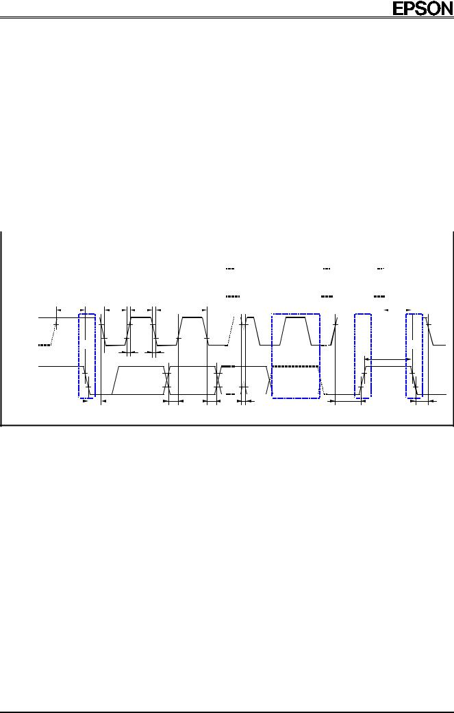
Timing chart |
|
|
|
|
|
|
Protocol
|
START |
|
BIT 7 |
BIT 6 |
|
|
BIT 0 |
ACK |
|
|
|
STOP |
|
START |
|
|
CONDITION |
|
MSB |
|
|
|
LSB |
|
|
|
|
CONDITION |
|
CONDITION |
|
|
(S) |
|
(A7) |
(A6) |
|
|
(R/W) |
(A) |
|
|
|
(P) |
|
(S) |
|
|
|
|
|
|
|
|
|
|
|
|
|
|
|
|
|
tSU ; STA |
|
tLOW |
tHIGH |
1 / fSCL |
|
|
|
|
tSU ; STA |
|
|
|||||||
|
|
|
|
|
|
|||||||||||||
|
|
|
|
|
|
|
|
|
|
|
|
|
|
|
|
|
|
|
|
|
|
|
|
|
|
|
|
|
|
|
|
|
|
|
|
|
|
|
|
|
|
|
|
|
|
|
|
|
|
|
|
|
|
|
|
|
SCL
(S) |
(P) |
(S) |
tr |
tf |
tBUF |
|
SDA
(A)
|
|
|
|
|
|
|
|
|
|
|
|
|
|
|
|
|
|
|
|
|
|
|
|
|
|
|
|
|
|
|
|
|
|
|
|
|
|
|
|
|
|
|
|
|
|
|
|
|
|
tHD ; STA |
|
tSU ; DAT |
tHD ; DAT |
|
|
tSP |
|
tSU ; STO |
|
|
tHD ; STA |
|||||||||||||
Caution: When accessing this device, all communication from transmitting the start condition to transmitting the stop condition after access should be completed within 0.95 seconds.
If such communication requires 0.95 seconds or longer, the I2C bus interface is reset by the internal bus timeout function.
Page - 4 |
MQ372-02 |

RX - 8581 SA / JE / NB
8. Use Methods
8.1. Overview of Functions
1) Clock functions
This function is used to set and read out month, day, hour, date, minute, second, and year (last two digits) data.
Any (two-digit) year that is a multiple of 4 is treated as a leap year and calculated automatically as such until the year 2099.
For details, see "8.2. Description of Registers".
2)Fixed-cycle interrupt generation function
The fixed-cycle timer interrupt generation function generates an interrupt event periodically at any fixed cycle set between 244.14 s and 4095 minutes.
When an interrupt event is generated, the /INT pin goes to low level ("L") and "1" is set to the TF bit to report that an event has occurred. (However, when a fixed-cycle timer interrupt event has been generated, low-level output from the /INT pin occurs only when the value of the control register's TIE bit is "1". Up to 7.8 ms after the interrupt occurs, the /INT status is automatically cleared (/INT status changes from low level to Hi-Z).
For details, see "8.3. Fixed-cycle Interrupt Function". .
3)Time update interrupt function
The time update interrupt function generates interrupt events at one-second or one-minute intervals, according to the timing of the internal clock.
When an interrupt event occurs, the UF bit value becomes "1" and the /INT pin goes to low level to indicate that an event has occurred. (However, when a fixed-cycle timer interrupt event has been generated, low-level output from the /INT pin occurs only when the value of the control register's UIE bit is "1". This /INT status is automatically cleared (/INT status changes from low level to Hi-Z) 7.8 ms (a fixed value) after the interrupt occurs.
For details, see "8.4. Time Update Interrupt Function".
4)Alarm interrupt function
The alarm interrupt generation function generates interrupt events for alarm settings such as date, day, hour, and minute settings.
When an interrupt event occurs, the AF bit value is set to "1" and the /INT pin goes to low level to indicate that an event has occurred.
For details, see "8.5. Alarm Interrupt Function".
5)32.768-kHz clock output
The 32.768-kHz clock (with precision equal to that of the built-in crystal oscillator) can be output via the FOUT pin. The FOUT pin is a CMOS output pin which can be set for clock output when the FOE pin is at high level and for low-level output when the FOE pin is at low level.
6) Interface with CPU
Data is read and written via the I2C bus interface using two signal lines: SCL (clock) and SDA (data).
Since neither SCL nor SDA includes a protective diode on the VDD side, a data interface between hosts with differing supply voltages can still be implemented by adding pull-up resistors to the circuit board.
The SCL's maximum clock frequency is 400 kHz (when VDD ≥ 1.8 V), which supports the I2C bus's high-speed mode.
For further description of data read/write operations, see "8.6 Reading/Writing Data via the I2C Bus Interface".
Page - 5 |
MQ372-02 |
RX - 8581 SA / JE / NB
8.2. Description of Registers
8.2.1. Register table
Address |
Function |
bit 7 |
bit 6 |
bit 5 |
bit 4 |
bit 3 |
bit 2 |
bit 1 |
bit 0 |
Remark |
||
|
|
|
|
|
|
|
|
|
|
|
|
|
0 |
SEC |
! |
40 |
20 |
10 |
8 |
4 |
2 |
1 |
|
3 |
|
1 |
MIN |
! |
40 |
20 |
10 |
8 |
4 |
2 |
1 |
|
3 |
|
2 |
HOUR |
! |
! |
20 |
10 |
8 |
4 |
2 |
1 |
|
3 |
|
3 |
WEEK |
! |
6 |
5 |
4 |
3 |
2 |
1 |
0 |
|
3 |
|
4 |
DAY |
! |
! |
20 |
10 |
8 |
4 |
2 |
1 |
|
3 |
|
5 |
MONTH |
! |
! |
! |
10 |
8 |
4 |
2 |
1 |
|
3 |
|
6 |
YEAR |
80 |
40 |
20 |
10 |
8 |
4 |
2 |
1 |
− |
|
|
7 |
RAM |
• |
• |
• |
• |
• |
• |
• |
• |
|
4 |
|
8 |
MIN Alarm |
AE |
40 |
20 |
10 |
8 |
4 |
2 |
1 |
− |
|
|
9 |
HOUR Alarm |
AE |
• |
20 |
10 |
8 |
4 |
2 |
1 |
|
4 |
|
A |
WEEK Alarm |
AE |
6 |
5 |
4 |
3 |
2 |
1 |
0 |
|
4 |
|
DAY Alarm |
• |
20 |
10 |
8 |
4 |
2 |
1 |
|||||
|
|
|
|
|||||||||
B |
Timer Counter 0 |
128 |
64 |
32 |
16 |
8 |
4 |
2 |
1 |
− |
|
|
C |
Timer Counter 1 |
• |
• |
• |
• |
2048 |
1024 |
512 |
256 |
|
4 |
|
D |
Extension Register |
TEST |
WADA USEL |
TE |
! |
! |
TSEL1 TSEL0 |
1, |
3, 5 |
|||
E |
Flag Register |
! |
! |
UF |
TF |
AF |
! |
VLF |
! |
1, |
2, 3 |
|
F |
Control Register |
! |
! |
UIE |
TIE |
AIE |
! |
STOP RESET |
|
3 |
||
Note When after the initial power-up or when the result of read out the VLF bit is "1" , initialize all registers, before using the module.
Be sure to avoid entering incorrect date and time data, as clock operations are not guaranteed when the data or time data is incorrect.
1) During the initial power-up, the TEST bit is reset to "0" and the VLF bit is set to "1".
At this point, all other register values are undefined, so be sure to perform a reset before using the module.
2) Only a "0" can be written to the UF, TF, AF, or VLF bit.
3) Any bit marked with "!" should be used with a value of "0" after initialization.
4) Any bit marked with "• " is a RAM bit that can be used to read or write any data.
5) The TEST bit is used by the manufacturer for testing. Be sure to set "0" for this bit when writing.
Page - 6 |
MQ372-02 |
RX - 8581 SA / JE / NB
8.2.2. Control register (Reg F)
Address |
Function |
bit 7 |
bit 6 |
bit 5 |
bit 4 |
bit 3 |
bit 2 |
bit 1 |
bit 0 |
|
|
|
|
|
|
|
|
|
|
|
|
F |
Control Register |
! |
! |
UIE |
TIE |
AIE |
! |
STOP |
RESET |
|
(Default) |
(0) |
(0) |
(− ) |
(− ) |
(− ) |
(0) |
(− ) |
(− ) |
||
|
1) The default value is the value that is read (or is set internally) after powering up from 0 V.
2) "o" indicates write-protected bits. A zero is always read from these bits.
3) "− " indicates no default value has been defined.
• This register is used to control interrupt event output from the /INT pin and the stop/start status of clock and calendar operations.
1) UIE (Update Interrupt Enable) bit
When a time update interrupt event is generated (when the UF bit value changes from "0" to "1"), this bit's value specifies if an interrupt signal is generated (/INT status changes from Hi-Z to low) or is not generated (/INT status remains Hi-Z).
When a "1" is written to this bit, an interrupt signal is generated (/INT status changes from Hi-Z to low) when an interrupt event is generated.
When a "0" is written to this bit, no interrupt signal is generated when an interrupt event occurs.
UIE |
Data |
Function |
|
0 |
When a time update interrupt event occurs, an interrupt signal is not |
|
generated or is canceled (/INT status changes from low to Hi-Z). |
|
|
|
|
|
|
|
Write/Read |
|
When a time update interrupt event occurs, an interrupt signal is generated |
|
(/INT status changes from Hi-Z to low). |
|
|
1 |
|
|
When a time update interrupt event occurs, low-level output from the /INT pin occurs only when |
|
|
|
the value of the control register's UIE bit is "1". This /INT status is automatically cleared (/INT |
|
|
status changes from low to Hi-Z) 7.8 ms after the interrupt occurs. |
For details, see "8.4. Time Update Interrupt Function".
2)TIE (Timer Interrupt Enable) bit
When a fixed-cycle timer interrupt event occurs (when the TF bit value changes from "0" to "1"), this bit's value specifies if an interrupt signal is generated (/INT status changes from Hi-Z to low) or is not generated (/INT status remains Hi-Z).
When a "1" is written to this bit, an interrupt signal is generated (/INT status changes from Hi-Z to low) when an interrupt event is generated.
When a "0" is written to this bit, no interrupt signal is generated when an interrupt event occurs.
TIE |
Data |
Function |
|
0 |
When a fixed-cycle timer interrupt event occurs, an interrupt signal is not |
|
generated or is canceled (/INT status changes from low to Hi-Z). |
|
|
|
|
|
|
|
Write/Read |
|
When a fixed-cycle timer interrupt event occurs, an interrupt signal is |
|
generated (/INT status changes from Hi-Z to low). |
|
|
1 |
|
|
* When a fixed-cycle timer interrupt event has been generated low-level output from the /INT pin |
|
|
|
occurs only when the value of the control register's TIE bit is "1". Up to 7.8 ms after the interrupt |
|
|
occurs, the /INT status is automatically cleared (/INT status changes from low to Hi-Z). |
For details, see "8.3. Fixed-cycle Timer Interrupt Function".
3)AIE (Alarm Interrupt Enable) bit
When an alarm timer interrupt event occurs (when the AF bit value changes from "0" to "1"), this bit's value specifies if an interrupt signal is generated (/INT status changes from Hi-Z to low) or is not generated (/INT status remains Hi-Z).
When a "1" is written to this bit, an interrupt signal is generated (/INT status changes from Hi-Z to low) when an interrupt event is generated.
When a "0" is written to this bit, no interrupt signal is generated when an interrupt event occurs.
AIE |
Data |
Function |
|
0 |
When an alarm interrupt event occurs, an interrupt signal is not generated |
|
or is canceled (/INT status changes from low to Hi-Z). |
|
|
|
|
|
|
|
Write/Read |
|
When an alarm interrupt event occurs, an interrupt signal is generated |
|
(/INT status changes from Hi-Z to low). |
|
|
1 |
|
|
When an alarm interrupt event has been generated low-level output from the /INT pin occurs |
|
|
|
only when the value of the control register's AIE bit is "1". This setting is retained until the AF bit |
|
|
value is cleared to zero. (No automatic cancellation) |
For details, see "8.5. Alarm Interrupt Function".
[Caution]
(1)The /INT pin is a shared interrupt output pin for three types of interrupts. It outputs the OR'ed result of these interrupt outputs.
When an interrupt has occurred (when the /INT pin is at low level), the UF, TF, read AF flags to determine which flag has a value of "1" (this indicates which type of interrupt event has occurred).
(2)To keep the /INT pin from changing to low level, write "0" to the UIE, TIE, and AIE bits. To check whether an event has occurred without outputting any interrupts via the /INT pin, use software to monitor the value of the UF, TF, and AF interrupt flags.
Page - 7 |
MQ372-02 |
 Loading...