


MQ162-03
Application Manual
Real Time Clock Module
RTC-72421/72423
Model |
Product Number |
RTC-72421 A |
Q4272421x000100 |
RTC-72421 B |
Q4272421x000200 |
RTC-72423 A |
Q4272423x000600 |
RTC-72423 |
Q4272423x000700 |

In pursuit of "Saving" Technology ,Epson electronic device.
Our Lineup of semiconductors, Liquid crystal displays and quartz devices assists in creating the products of our customers' dreams.
Epson IS energy savings.
NOTICE
•The material is subject to change without notice.
•Any part of this material may not be reproduced or duplicated in any form or any means without the written permission of Seiko Epson.
•The information, applied circuit, program, using way etc., written in this material is just for reference. Seiko Epson does not assume any liability for the occurrence of infringing any patent or copyright of third party. This material does not authorize the licence for any patent or intellectual property rights.
•Any product described in this material may contain technology or the subject relating to strategic products under the control of the Foreign Exchange and Foreign Trade Law of Japan and may require an export licence from the Ministry of International Trade and industry or other approval from another government agency.
•The products (except for some product for automotive applications) listed up on this material are designed to be used with ordinary electronic equipment (OA equipment, AV equipment, communications equipment, measuring instruments etc). Seiko Epson does not assume any liability for the case using the products with the appoication required high reliability or safety extremely (such as aerospace equipment etc).
When intending to use any our product with automotive application and the other application than ordinary electronic equipments as above, please contact our sales representatives in advance.

RTC - 72421 / 72423
|
CONTENTS |
|
Overview ............................................................................................. |
1 |
|
Block diagram ..................................................................................... |
1 |
|
Terminal connections.......................................................................... |
2 |
|
Terminal functions............................................................................... |
3 |
|
Characteristics .................................................................................... |
4 |
|
1. |
Absolute maximum ratings........................................................................................ |
4 |
2. |
Recommended operating conditions......................................................................... |
4 |
3. |
Frequency characteristics and current consumption characteristics.......................... |
4 |
4. |
Electrical characteristics ( DC characteristics ) ......................................................... |
4 |
Switching characteristics (AC characteristics) ........................................... |
5 |
|
1. |
When ALE is used .................................................................................................... |
5 |
2. |
When ALE is fixed at VDD ......................................................................................... |
6 |
Registers............................................................................................. |
7 |
|
1. |
Register table............................................................................................................ |
7 |
2. |
Notes ........................................................................................................................ |
7 |
3. |
Functions of register bits (overview).......................................................................... |
7 |
4. |
Setting the fixed-period pulse output mode and fixed-period interrupt mode............. |
8 |
5. |
Resetting the fixed-period pulse output mode and fixed-period interrupt mode......... |
8 |
Register description ............................................................................ |
9 |
|
1. |
Timing registers ........................................................................................................ |
9 |
2. |
CD register (control register D) ............................................................................... |
10 |
3. |
CE register (control register E)................................................................................ |
11 |
4. |
CF register (control register F) ................................................................................ |
13 |
Using the RTC-72421/RTC-72423 ..................................................... |
14 |
|
1. |
Power-on procedure (initialization) .......................................................................... |
14 |
2. |
Read/write of S1 to W registers .............................................................................. |
16 |
3. |
Write to 30-second ADJ bit ..................................................................................... |
16 |
4. |
Using the CS1 pin ................................................................................................... |
17 |
Power supply circuit example............................................................. |
17 |
|
Examples of connection to general-purpose microprocessor............. |
18 |
|
External dimensions........................................................................... |
19 |
|
Marking layout.................................................................................... |
19 |
|
Reference data .................................................................................. |
20 |
|
Application notes................................................................................ |
21 |
|
1. |
Notes on handling ................................................................................................... |
21 |
2. |
Notes on packaging ................................................................................................ |
21 |

RTC - 72421 / 72423
4-BIT PARALLEL INTERFACE REAL TIME CLOCK MODULE
RTC - 72421 / 72423
•Built-in crystal unit removes need for adjustment and reduces installation costs
•Microprocessor bus compatible ( tWW, tRD = 120 ns )
•Use of C-MOS IC enables low current consumption ( 5 A Max., at VDD = 2.0 V )
•Compatibility with Intel CPU bus
•Address latch enable (ALE) pin compatible with multiplex bus CPUs
•Time (hours, minutes, seconds) and calendar (year, month, day) counter
•24-hour/12-hour switchover and automatic leap-year correction functions
•Fixed-period interrupt function
•30-seconds correction (adjustment) function
•Stop, start, and reset functions
•Battery back-up function
•Same mounting conditions as general-purpose SMD ICs possible (RTC-72423)
Pins and functions compatible with the SMC-5242 series
Overview
The RTC-72421/RTC-72423 module is a real time clock that can be connected directly to a microprocessor's bus. Its built-in crystal unit enables highly accurate time-keeping with no physical access required for adjustment and, since there is no need to connect external components, mounting and other costs can be reduced.
In addition to its time and calendar functions, the RTC-72421/RTC-72423 enables the use of 30-seconds correction and fixedperiod interrupt functions.
The RTC-72421/RTC-72423 module is ideally suited for applications requiring timing management, such as personal computers, dedicated word-processors, fax machines, multi-function telephones, and sequencers.
Block diagram |
|
|
|
|
|
|
|
|
|
|
|
|
|
|
|
|
RTC-72421/72423 |
||
|
|
OSC |
Counter |
|
|
|
|
|
|
D3 |
|
RESET |
STOP |
|
HOLD |
BUSY |
|
|
|
D2 |
Gate |
|
|
|
|
||||
bit |
bit |
|
bit |
bit |
|
24/12 |
|||
D1 |
|
|
|||||||
|
30sec ADJ |
|
|
|
|
|
bit |
|
|
D0 |
|
|
|
|
|
|
|
||
|
|
|
|
|
|
|
|
||
|
|
bit |
|
|
|
|
|
|
|
WR |
|
|
S1 |
S10 |
MI1 |
MI10 |
H1 |
H10 |
W |
Gate |
|
|
|
|
|
|
|
|
|
RD |
|
|
|
|
|
|
|
|
|
|
|
|
|
|
|
|
|
|
|
A3 |
|
S1 to CF |
|
|
|
|
|
|
|
A2 |
|
D1 |
D10 |
MO1 |
MO10 |
Y1 |
Y10 |
|
|
A1 |
Latch |
Decoder |
|
||||||
|
|
|
|
|
|
|
|||
A0 |
|
|
|
|
|
|
|
|
|
CS0 |
|
|
|
|
|
|
|
|
|
|
|
|
|
|
|
|
|
|
Output Selector |
ALE |
|
|
|
|
|
|
|
|
STD.P |
|
|
|
|
|
|
|
|
64 Hz |
|
CS1 |
|
|
|
|
|
|
|
|
|
|
|
|
|
|
|
1 Second carry |
|
||
|
|
|
|
|
|
|
|
||
|
|
|
CD |
|
CE |
CF |
1 Minute carry |
|
|
|
|
|
|
1 Hour carry |
|
||||
|
|
|
|
|
|
|
|
||
Page - 1 |
MQ - 162 - 03 |
RTC - 72421 / 72423
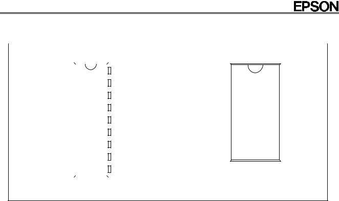
Terminal connections
|
|
|
|
|
RTC-72421 |
|
|
|
|
|
|
|
|
|
|
RTC-72423 |
|
|
|
|||||||||
STD.P |
1 |
|
|
|
|
|
18 |
VDD |
|
STD.P |
1 |
|
|
|
|
|
|
24 |
|
VDD |
||||||||
|
|
|
|
|
|
|
|
|
|
|
|
|
||||||||||||||||
|
|
|
|
|
|
|
|
|
2 |
|
|
|
|
|
23 |
(VDD) |
||||||||||||
|
|
|
|
2 |
|
|
|
|
|
17 |
(VDD) |
|
CS0 |
|
|
|
|
|
|
|||||||||
|
|
|
|
|
|
|
|
|
|
|
|
|
||||||||||||||||
|
CS0 |
|
|
|
|
|
|
|
|
|
|
N.C. |
3 |
|
|
|
|
|
22 |
(VDD) |
||||||||
ALE |
3 |
|
|
|
|
|
16 |
(VDD) |
|
ALE |
4 |
|
|
|
|
21 |
|
N.C. |
||||||||||
|
|
|
|
|
|
A0 |
5 |
|
|
|
|
|
20 |
|
CS1 |
|||||||||||||
A0 |
4 |
|
|
|
|
|
15 |
CS1 |
|
|
|
|
|
|
|
|||||||||||||
|
|
|
|
|
|
|
|
|
||||||||||||||||||||
|
|
|
|
|
|
N.C. |
6 |
|
|
|
|
|
19 |
|
D0 |
|||||||||||||
|
|
|
|
|
|
|
|
|
|
|
||||||||||||||||||
|
|
|
|
|
|
|
|
|
||||||||||||||||||||
A1 |
5 |
|
|
|
|
|
14 |
D0 |
|
A1 |
7 |
|
|
|
|
18 |
|
N.C. |
||||||||||
|
|
|
|
|
|
|
|
|
|
|||||||||||||||||||
|
|
|
|
|
|
N.C. |
8 |
|
|
|
|
|
17 |
|
N.C. |
|||||||||||||
|
|
|
|
|
|
|
|
|
|
|
|
|
|
|
|
|
|
|
|
|
||||||||
|
|
|
|
|
|
|
|
|
|
|
|
|
|
|
|
|
|
|||||||||||
A2 |
6 |
|
|
|
|
|
13 |
D1 |
|
A2 |
9 |
|
|
|
|
|
16 |
|
D1 |
|||||||||
A3 |
7 |
|
|
|
|
|
12 |
D2 |
|
A3 |
10 |
|
|
|
|
15 |
|
D2 |
||||||||||
|
|
|
|
|
|
|
|
|
|
|||||||||||||||||||
|
|
|
|
|
|
|
|
|
|
|
|
|
|
|
|
|
|
|
|
|||||||||
|
|
|
|
|
|
RD |
11 |
|
|
|
|
|
14 |
|
D3 |
|||||||||||||
|
|
|
|
|
|
|
|
|
|
|
|
|
|
|
GND |
12 |
|
|
|
|
|
13 |
|
|
|
|||
|
RD |
|
|
8 |
|
|
|
|
|
11 |
D3 |
|
|
|
|
|
|
|
WR |
|
||||||||
|
|
|
|
|
|
|
|
|
|
|
|
|||||||||||||||||
GND |
9 |
|
|
|
|
|
10 |
|
|
|
|
|
|
|
|
|
|
|
|
|
|
|
|
|
|
|||
|
|
|
|
|
|
WR |
|
|
|
|
|
|
|
|
|
|
|
|
|
|
|
|
||||||
|
|
|
|
|
|
|
|
|
|
|
|
|
|
|
|
|
|
|
|
|
|
|
|
|
|
|
|
|
|
|
|
|
|
|
|
|
|
|
|
|
|
|
|
|
|
|
|
|
|
|
|
|
|
|
|
|
|
|
|
|
|
|
|
|
|
|
|
|
|
|
|
|
|
|
|
|
|
|
|
|
|
|
|
|
|
|
The (VDD) pins are at the same electrical level as VDD. Do not connect these pins externally. The N.C. pins are not connected internally. Ground them in order to prevent noise.
Page - 2 |
MQ - 162 - 03 |
RTC - 72421 / 72423
Terminal functions
Signal |
|
Pin No. |
Input/ou |
|
|
|
|
|
|
|
|
|
|
|
|
|
|
|
|
|
|
|
|
|
|
|
|
Function |
|
|
|
|
|
|
|
|
|
|
||||||||||||||||||
|
|
|
tput |
|
|
|
|
|
|
|
|
|
|
|
|
|
|
|
|
|
|
|
|
|
|
|
|
|
|
|
|
|
|
|
|
|
|
|||||||||||||||||||
|
|
|
|
|
|
RTC-72421 |
RTC-72423 |
|
|
|
|
|
|
|
|
|
|
|
|
|
|
|
|
|
|
|
|
|
|
|
|
|
|
|
|
|
|
|
|
|
|
|
|
|
|
|
|
|
|
|
|
|
|
|||
|
|
|
|
|
|
|
|
|
|
|
|
|
|
|
|
|
|
|
|
|
|
|
|
|
|
|
|
|
|
|
|
|
|
|
|
|
|
|
|
|
|
|
|
|||||||||||||
|
|
|
|
|
|
|
|
|
|
Connect these pines to a bi-directional data bus or CPU data bus. Use this bus |
||||||||||||||||||||||||||||||||||||||||||||||
|
|
|
|
|
|
|
|
|
|
to read to and write from the internal counter and registers. |
|
|
|
|
|
|
|
|||||||||||||||||||||||||||||||||||||||
|
|
|
|
|
|
|
|
|
|
|
|
|
|
|
|
|
|
|
|
|
|
|
|
|
|
|
|
|
|
|
|
|
|
|
|
|
|
|
|
|
|
|
|
|
|
|
|
|
|
|
|
|
||||
|
|
|
|
|
|
|
|
|
|
|
|
CS1 |
|
CS0 |
|
RD |
|
|
|
WR |
|
|
|
|
|
|
|
|
|
|
|
|
|
|
Mode of D0 to D3 |
|
|
|
|
|
|
|
||||||||||||||
D0-D3 |
11− |
|
14− 16, 19 |
Bi- |
|
|
|
H |
|
|
L |
|
|
|
L |
|
|
|
|
H |
|
|
|
|
|
|
|
|
Output mode (read mode) |
|
|
|
|
|
||||||||||||||||||||||
14 |
|
|
|
H |
|
|
L |
|
|
|
H |
|
|
|
|
L |
|
|
|
|
|
|
|
|
Input mode (write mode) |
|
|
|
|
|
||||||||||||||||||||||||||
(Data bus) |
direction |
|
|
|
|
|
|
|
|
|
|
|
|
|
|
|
|
|
|
|
|
|
|
|
|
|
||||||||||||||||||||||||||||||
|
|
|
|
|
|
|
|
|
|
|
|
|
H |
|
|
L |
|
|
|
L |
|
|
|
|
L |
|
|
|
|
|
|
|
|
|
|
|
|
|
Do not use |
|
|
|
|
|
|
|
||||||||||
|
|
|
|
|
|
|
|
|
|
|
|
|
L |
|
|
|
|
H or L |
|
|
|
|
High impedance (back-up mode) |
|
||||||||||||||||||||||||||||||||
|
|
|
|
|
|
|
|
|
|
|
|
|
H |
|
|
H |
|
|
|
H or L |
|
|
|
|
High impedance (RTC not selected) |
|
||||||||||||||||||||||||||||||
|
|
|
|
|
|
|
|
|
|
|
|
|
|
|
|
|
|
|
|
|
|
|
|
|
|
|
|
|
|
|
|
|
|
|
|
|
|
|
|
|
|
|
|
|||||||||||||
|
|
|
|
|
|
|
|
|
|
Address input pins used for connection to CPU address, etc. Used to select the |
||||||||||||||||||||||||||||||||||||||||||||||
A0-A3 |
4− |
7 |
5, 7, 9, 10 |
Input |
RTC’s internal counter and registers (address selection). |
|
|
|
|
|
|
|
||||||||||||||||||||||||||||||||||||||||||||
(Address bus) |
When the RTC is connected to a multiplexed-bus type of CPU, these pines can |
|||||||||||||||||||||||||||||||||||||||||||||||||||||||
|
|
|
|
|||||||||||||||||||||||||||||||||||||||||||||||||||||
|
|
|
|
|
|
|
|
|
|
also be used in combination with the ALE described below |
|
|
|
|
|
|
|
|||||||||||||||||||||||||||||||||||||||
|
|
|
|
|
|
|
|
|
|
|
|
|
|
|
|
|
|
|
|
|
|
|
|
|
|
|
|
|
|
|
|
|
|
|
|
|
|
|||||||||||||||||||
|
|
|
|
|
|
|
|
|
|
Reads in address data and |
|
|
|
|
state for internal latching. |
|
|
|
|
|
|
|
||||||||||||||||||||||||||||||||||
|
|
|
|
|
|
|
|
|
|
CS0 |
|
|
|
|
|
|
|
|||||||||||||||||||||||||||||||||||||||
|
|
|
|
|
|
|
|
|
|
When the ALE is high, the address data and |
|
|
|
|
state is read into the RTC. |
|||||||||||||||||||||||||||||||||||||||||
|
|
|
|
|
|
|
|
|
|
CS0 |
|
|||||||||||||||||||||||||||||||||||||||||||||
|
|
|
|
|
|
|
|
|
|
When the (through-mode) ALE falls, the address data and |
|
|
|
state at that |
||||||||||||||||||||||||||||||||||||||||||
|
|
|
|
|
|
|
|
|
|
CS0 |
||||||||||||||||||||||||||||||||||||||||||||||
|
ALE |
|
|
|
|
point are held. The held address data and |
|
|
|
status are maintained while |
||||||||||||||||||||||||||||||||||||||||||||||
|
3 |
|
4 |
Input |
CS0 |
|||||||||||||||||||||||||||||||||||||||||||||||||||
(Address Latch Enable) |
|
the ALE is low. |
|
|
|
|
|
|
|
|
|
|
|
|
|
|
|
|
|
|
|
|
|
|
|
|
|
|
|
|
|
|
|
|
|
|
|
|
|
|
||||||||||||||||
|
|
|
|
|
|
|
|
|
|
|
|
|
|
|
|
|
|
|
|
|
|
|
|
|
|
|
|
|
|
|
|
|
|
|
|
|
|
|
|
|
|
|||||||||||||||
|
|
|
|
|
|
|
|
|
|
|
|
|
|
|
|
|
|
|
|
|
|
|
|
|
|
|
|
|
|
|
|
|
|
|
|
|
|
|
|
|
|
|
|
|
|
|
|
|
|
|
||||||
|
|
|
|
|
|
|
|
|
|
|
|
|
ALE |
|
|
|
|
|
|
|
|
|
|
|
|
|
|
Address data and |
CS0 |
status |
|
|
|
|
|
|
|
|||||||||||||||||||
|
|
|
|
|
|
|
|
|
|
|
|
|
H |
Read into the RTC to set address data |
|
|
|
|
|
|
|
|||||||||||||||||||||||||||||||||||
|
|
|
|
|
|
|
|
|
|
|
|
|
L |
Held in the RTC (latched at the trailing edge of the ALE) |
|
|
||||||||||||||||||||||||||||||||||||||||
|
|
|
|
|
|
|
|
|
|
If the RTC is connected to a CPU that does not have an ALE pin and thus there |
||||||||||||||||||||||||||||||||||||||||||||||
|
|
|
|
|
|
|
|
|
|
is no need to use this ALE pin, fix it to VDD. |
|
|
|
|
|
|
|
|
|
|
||||||||||||||||||||||||||||||||||||
|
|
|
|
|
|
|
|
|
|
|
|
|
|
|
|
|
|
|
|
|
|
|
|
|
|
|
|
|
|
|
||||||||||||||||||||||||||
|
|
|
|
|
|
|
|
|
|
Writes the data on D0 to D3 into the register of the address specified by A0 to |
||||||||||||||||||||||||||||||||||||||||||||||
|
|
|
|
|
|
|
|
|
|
|
|
|
|
|
|
|
|
|
|
|
|
|
|
|
|
|
|
|
|
|
|
|
|
|
|
|
|
|
|
|
||||||||||||||||
|
WR |
|
|
|
|
A3, at the leading edge of |
|
|
|
. |
|
|
|
|
|
|
|
|
|
|
|
|
|
|
|
|
|
|
|
|||||||||||||||||||||||||||
|
10 |
13 |
Input |
WR |
|
|
|
|
|
|
|
|
|
|
||||||||||||||||||||||||||||||||||||||||||
(WRite) |
|
|
|
|
|
|
|
|
|
|
|
|
|
|
|
|
|
|
|
|
|
|
|
|
|
|
|
|
|
|
|
|
|
|
|
|
|
|
|
|
|
|
|
|
|
|
||||||||||
|
|
|
|
Make sure that |
|
|
|
|
|
|
|
|
|
|
|
|
|
|
|
|
|
|
|
|
|
|
|
|
|
|
|
|
|
|
|
|
|
|
|
|
|
|
||||||||||||||
|
|
|
|
|
|
RD |
and |
WR are never low at the same time. |
||||||||||||||||||||||||||||||||||||||||||||||||
|
|
|
|
|
|
|
|
|
|
|
|
|||||||||||||||||||||||||||||||||||||||||||||
|
|
|
|
|
|
|
|
|
|
|
|
|
|
|
|
|
|
|
|
|
|
|
|
|
|
|
|
|
||||||||||||||||||||||||||||
|
|
|
|
|
|
|
|
|
|
Output data to D0 to D3 from the register at the address specified by A0 to A3, |
||||||||||||||||||||||||||||||||||||||||||||||
|
|
|
|
|
|
|
|
|
|
|
|
|
|
|
|
|
|
|
|
|
|
|
|
|
|
|
|
|
|
|
|
|
|
|
|
|
|
|
|
|
|
|
|
|
|
|
|
|
||||||||
|
RD |
|
|
|
|
while |
|
|
is |
low. |
|
|
|
|
|
|
|
|
|
|
|
|
|
|
|
|
|
|
|
|
|
|
|
|
|
|
|
|
|
|
|
|
|
|||||||||||||
|
8 |
|
11 |
Input |
|
RD |
|
|
|
|
|
|
|
|
|
|
|
|
|
|
|
|
|
|
|
|
|
|
|
|
|
|
|
|
|
|
|
|
|
|
||||||||||||||||
(ReaD) |
|
|
|
|
|
|
|
|
|
|
|
|
|
|
|
|
|
|
|
|
|
|
|
|
|
|
|
|
|
|
|
|
|
|
|
|
|
|
|
|
|
|
|
|
|
|
|
|||||||||
|
|
|
|
Make sure that |
|
|
|
|
|
|
|
|
|
|
|
|
|
|
|
|
|
|
|
|
|
|
|
|
|
|
|
|
|
|
|
|
|
|
|
|
|
|
||||||||||||||
|
|
|
|
|
|
RD |
and |
WR are never low at the same time. |
||||||||||||||||||||||||||||||||||||||||||||||||
|
|
|
|
|
|
|
|
|
|
|
|
|||||||||||||||||||||||||||||||||||||||||||||
|
|
|
|
|
|
|
|
|
|
|
|
|
|
|
|
|
|
|
|
|
|
|
|
|
|
|
||||||||||||||||||||||||||||||
|
|
|
|
|
|
|
|
|
|
When CS1 is high and |
|
|
|
|
is low, the RTC’s chip-select function is valid and |
|||||||||||||||||||||||||||||||||||||||||
|
|
|
|
|
|
|
|
|
|
CS0 |
||||||||||||||||||||||||||||||||||||||||||||||
|
|
|
|
|
|
|
|
|
|
read and write are enabled. |
|
|
|
|
|
|
|
|
|
|
|
|
|
|
|
|
|
|
|
|
|
|
|
|
|
|
||||||||||||||||||||
|
|
|
|
|
|
|
|
|
|
When the RTC is connected to a multiplexed-bus type of CPU, |
|
|
|
requires |
||||||||||||||||||||||||||||||||||||||||||
CS1, |
|
|
|
|
|
|
|
|
|
CS0 |
||||||||||||||||||||||||||||||||||||||||||||||
CS0 |
|
15,2 |
20,2 |
Input |
the operation of the ALE (see the description of the ALE). |
|
|
|
|
|
|
|
||||||||||||||||||||||||||||||||||||||||||||
(Chip Select) |
|
|
|
|
|
|
|
|||||||||||||||||||||||||||||||||||||||||||||||||
|
|
|
|
Use CS1 connected to a power voltage detection circuit. When CS1 is high, the |
||||||||||||||||||||||||||||||||||||||||||||||||||||
|
|
|
|
|
|
|
|
|
|
RTC is enabled; when it is low, the RTC is on standby. |
|
|
|
|
|
|
|
|||||||||||||||||||||||||||||||||||||||
|
|
|
|
|
|
|
|
|
|
When CS1 goes low, the HOLD and RESET bits in the RTC registers are |
||||||||||||||||||||||||||||||||||||||||||||||
|
|
|
|
|
|
|
|
|
|
cleared to 0. |
|
|
|
|
|
|
|
|
|
|
|
|
|
|
|
|
|
|
|
|
|
|
|
|
|
|
|
|
|
|
|
|
|
|
|
|
|
|
||||||||
|
|
|
|
|
|
|
|
|
|
|
|
|
|
|
|
|
|
|
|
|
||||||||||||||||||||||||||||||||||||
|
|
|
|
|
|
|
|
|
|
This is an N-channel open drain output pin. |
|
|
|
|
|
|
|
|
|
|
||||||||||||||||||||||||||||||||||||
|
|
|
|
|
|
|
|
|
|
Depending on the setting of the CE register, a fixed-period interrupt signal and a |
||||||||||||||||||||||||||||||||||||||||||||||
|
|
|
|
|
|
|
|
|
|
pulse signal are output. |
|
|
|
|
|
|
|
|
|
|
|
|
|
|
|
|
|
|
|
|
|
|
|
|
|
|
||||||||||||||||||||
|
|
|
|
|
|
|
|
|
|
The output from this pin cannot be inhibited by the CS1 and |
|
|
signals. |
|||||||||||||||||||||||||||||||||||||||||||
|
|
|
|
|
|
|
|
|
|
CS0 |
|
|||||||||||||||||||||||||||||||||||||||||||||
|
|
|
|
|
|
|
|
|
|
Use a load voltage that is less than or equal to VDD. If not using this pin, keep it |
||||||||||||||||||||||||||||||||||||||||||||||
|
|
|
|
|
|
|
|
|
|
open-circuit. |
|
|
|
|
|
|
|
|
|
|
|
|
|
|
|
|
|
|
|
|
|
|
|
|
|
|
|
|
|
|
|
|
|
|
|
|
|
|
|
|
||||||
|
|
|
|
|
|
|
|
|
|
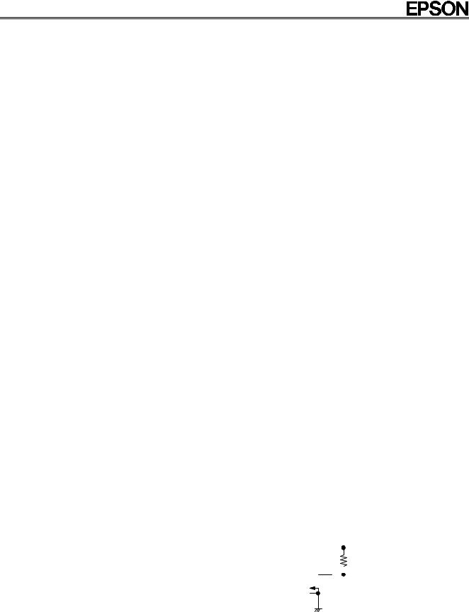
An example of STD.P connection is shown below. |
|
|
|
|
|
|
|
|
|
|
||||||||||||||||||||||||||||||||||||
|
|
|
|
|
|
|
|
|
|
|
|
|
|
|
|
|
|
|
|
|
|
|
|
|
|
|
|
|
|
|
|
|
|
|
|
|
|
|
|
|
|
+5 V or VDD |
|
|
|
|
|
|
|
|||||||
STD.P |
|
|
|
|
|
|
|
|
|
|
|
|
|
|
|
|
|
RTC |
|
|
|
|
|
|
|
|
|
|
|
|
At least 2.2 kΩ |
|
|
|
|
|
|
|
||||||||||||||||||
1 |
|
1 |
Output |
|
|
|
|
|
|
|
|
|
|
|
|
|
|
|
|
|
|
|
|
|
|
|
|
|
|
|
|
|
|
|
|
|
|
|
|
|
|
|
||||||||||||||
(STanDard Pulse) |
|
|
|
|
|
|
|
|
|
|
|
|
|
|
|
|
|
|
|
|
|
|
|
|
|
|
|
|
|
|
|
|
|
|
|
|
|
|
|
|
|
|
|
|
|
|
|
|||||||||
|
|
|
|
|
|
|
|
|
|
|
|
|
|
|
|
|
|
|
|
|
|
|
|
|
|
|
|
|
|
|
|
|
|
|
|
|
|
|
|
|
|
|
|
|
|
|
|
|
|
|||||||
|
|
|
|
|
|
|
|
|
|
|
|
|
|
|
|
|
|
|
|
|
|
|
|
|
|
|
|
|
|
|
|
|
|
|
|
|
STD.P |
|
|
|
|
|
|
|
|
|
|
|||||||||
|
|
|
|
|
|
|
|
|
|
|
|
|
|
|
|
|
|
|
|
|
|
|
|
|
|
|
|
|
|
|
|
|
|
|
|
|
|
|
|
|
|
|
|
|
|
|
|
|
|
|
|
|
|
|
|
|
|
|
|
|
|
|
|
|
|
|
|
|
|
|
|
|
|
|
|
|
|
|
|
|
|
|
|
|
|
|
|
|
|
|
|
|
|
|
|
|
|
|
|
|
|
|
|
|
|
|
|
|
|
|
|
|
|
|
|
|
|
|
|
|
|
|
|
If the STD.P output is not be used during standby operation, connecting the pull- |
||||||||||||||||||||||||||||||||||||||||||||||
|
|
|
|
|
|
|
|
|
|
up resister to +5 V provides a reduction in current consumption. If the STD.P |
||||||||||||||||||||||||||||||||||||||||||||||
|
|
|
|
|
|
|
|
|
|
output is to be used even during standby, connect the pull-up resistor to the |
||||||||||||||||||||||||||||||||||||||||||||||
|
|
|
|
|
|
|
|
|
|
RTC’s VDD. In this case, the current consumption will be increased by the |
||||||||||||||||||||||||||||||||||||||||||||||
|
|
|
|
|
|
|
|
|
|
amount of current flowing through the pull-up resistor. |
|
|
|
|
|
|
|
|||||||||||||||||||||||||||||||||||||||
|
|
|
|
|
|
|
|
|
|
|
|
|||||||||||||||||||||||||||||||||||||||||||||
|
VDD |
18 |
24 |
|
Connect this pin to power source. Supply to 5 V ± |
10 % to this pin during normal |
||||||||||||||||||||||||||||||||||||||||||||||||||
|
|
operation; at least 2 V during battery back-up operation. |
|
|
|
|
|
|
|
|||||||||||||||||||||||||||||||||||||||||||||||
|
|
|
|
|
|
|
|
|
|
|
|
|
|
|
|
|
||||||||||||||||||||||||||||||||||||||||
|
|
|
|
|
|
|
|
|
|
|
|
|
|
|
|
|
|
|
|
|
|
|
|
|
|
|
|
|
|
|
|
|||||||||||||||||||||||||
GND |
9 |
|
12 |
|
Connect this pin to ground. |
|
|
|
|
|
|
|
|
|
|
|
|
|
|
|
|
|
|
|
|
|
|
|
|
|
|
|||||||||||||||||||||||||
|
|
|
|
|
||||||||||||||||||||||||||||||||||||||||||||||||||||
(VDD) |
16, 17 |
22,23 |
|
These pins are connected internally to VDD. Leave them open circuit. |
||||||||||||||||||||||||||||||||||||||||||||||||||||
|
|
|
|
|
|
|
|
|
|
|
|
|
|
|
|
|
|
|
|
|
|
|
|
|
|
|
|
|
|
|
|
|
|
|
|
|
|
|
|
|
|
|
|
|
|
|
|
|
|
|
|
|
|
|
|
|
|
N.C. |
− |
|
3, 6, 8, |
|
These pins are not connected internally. Ground them. |
|
|
|
|
|
|
|
|||||||||||||||||||||||||||||||||||||||||||
|
|
17, 18, 21 |
|
|
|
|
|
|
|
|
||||||||||||||||||||||||||||||||||||||||||||||
|
|
|
|
|
|
|
|
|
|
|
|
|
|
|
|
|
|
|
|
|
|
|
|
|
|
|
|
|
|
|
|
|
|
|
|
|
|
|
|
|
|
|
|
|
|
|
|
|
|
|
|
|
|
|
||
|
|
|
|
|
|
|
|
|
|
|
|
|
|
|
|
|
|
|
|
|
|
|
|
|
|
|
|
|
|
|
|
|
|
|
|
|
|
|
|
|
|
|
|
|
|
|
|
|
|
|
|
|
|
|
|
|
Page - 3 |
MQ - 162 - 03 |

RTC - 72421 / 72423
Characteristics
1. Absolute maximum ratings
Item |
Symbol |
Condition |
|
|
Specification |
Unit |
|||||||||
Supply voltage |
VDD |
Ta=+25 ° C |
|
|
|
− 0.3 |
to |
|
7.0 |
|
|
|
V |
||
Input voltage |
VI |
Ta=+25 ° C |
|
GND− 0.3 |
to |
|
VDD+0.3 |
|
V |
||||||
Output voltage |
VO |
Ta=+25 ° C |
|
GND− 0.3 |
to |
|
VDD+0.3 |
|
V |
||||||
Storage temperature |
TSTG |
RTC-72421 |
|
|
|
− 55 |
to |
|
+85 |
|
|
° C |
|||
RTC-72423 |
|
|
|
− 55 |
to |
|
+125 |
|
|
° C |
|||||
|
|
|
|
|
|
|
|
||||||||
2. Recommended operating conditions |
|
|
|
|
|
|
|
|
|
|
|
|
|||
|
|
|
|
|
|
|
|
|
|
|
|||||
Item |
Symbol |
Condition |
|
|
Specification |
|
Unit |
||||||||
Supply voltage |
VDD |
|
|
|
|
4.5 |
to |
5.5 |
|
|
|
|
V |
||
|
|
|
|
|
|
|
|
|
|
|
|
||||
Operating temperature |
TOPR |
No condensation |
|
RTC-72421 ; − |
10 to +70 |
|
|
° C |
|||||||
|
RTC-72423 ; − 40 to +85 |
|
|
° C |
|||||||||||
|
|
|
|
|
|
|
|||||||||
Data hold voltage |
VDH |
|
|
|
|
2.0 |
to |
5.5 |
|
|
|
|
V |
||
CS1 data hold time |
tCDR |
See the section on data |
|
|
|
2.0 Min. |
|
|
|
|
|
µ s |
|||
|
|
hold timing |
|
|
|
|
|
|
|
|
|||||
Operation recovery time |
tr |
|
|
|
|
|
|
|
|||||||
|
|
|
|
|
|
|
|
|
|
|
|
||||
|
|
|
|
|
|
|
|
|
|
|
|
|
|||
3. Frequency characteristics and current consumption characteristics |
|
|
|
|
|
|
|
||||||||
Item |
Symbol |
Condition |
|
|
Specification |
|
Unit |
||||||||
|
|
|
|
RTC-72421A |
|
|
|
|
± |
10 |
|
|
|
||
Frequency tolerance |
∆ f/f0 |
Ta=+25 ° C |
|
RTC-72421B |
|
|
|
|
± |
50 |
|
|
|
||
VDD=5.0 V |
|
RTC-72423A |
|
|
|
|
± |
20 |
|
|
|
||||
|
|
|
|
|
|
|
|
|
|
||||||
|
|
|
|
|
RTC-72423 |
|
|
|
|
± |
50 |
|
× |
-6 |
|
|
|
|
|
|
|
|
|
|
|
|
|
|
|
10 |
|
|
|
RTC-72421 : − 10 ° C to +70 ° C |
|
|
|
+10 / − 120 |
|
||||||||
|
|
|
|
|
|
|
|
||||||||
|
|
(+25 ° C reference) |
|
|
|
|
|
|
|||||||
Operation temperature |
|
|
|
|
|
|
|
|
|
|
|
||||
|
RTC-72423 : − 40 ° C to +85 ° C |
|
|
|
+10 / − 220 |
|
|
|
|||||||
|
|
|
|
|
|
|
|
||||||||
|
|
(+25 ° C reference) |
|
|
|
|
|
|
|||||||
|
|
|
|
|
|
|
|
|
|
|
|
||||
Frequency voltage |
|
Ta=+25 ° C |
|
|
|
± |
5 Max. |
|
× 10-6 / V |
||||||
characteristics |
|
|
|
|
|
||||||||||
|
VDD=2.0 V to 5.5 V |
|
|
|
|
|
|
|
|
|
|
||||
Aging |
fa |
VDD=5.0 V, Ta=+25 ° C |
|
|
|
± |
5 Max. |
|
× 10-6 / year |
||||||
|
|
Drop test 3 times on a hard board from |
|
|
|
|
|
|
|
|
|
||||
Shock resistance |
S.R. |
0.75 m height, or 29400 m/s2 × 0.2 ms × |
|
|
± |
10 Max. |
|
× |
10-6 |
||||||
|
|
1/2 sin wave × 3 directions |
|
|
|
|
|
|
|
|
|
|
|||
Current consumption |
IDD1 |
Ta=+25 ° C, CS1=0 V |
|
|
VDD=5.0 V |
|
1.0 Typ. |
|
10 Max. |
|
|
µ A |
|||
IDD2 |
I/O currents excluded |
|
|
VDD=2.0 V |
|
0.9 Typ. |
|
5 Max. |
|
|
|||||
|
|
|
|
|
|
|
|
||||||||
|
|
|
|
|
|
|
|
|
|
|
|
|
|
|
|
4. Electrical characteristics ( DC characteristics )
Item |
Symbol |
Condition |
Applicable pins |
Min. |
Typ. |
Max. |
Unit |
|
|
|
|
|
|
|
|
High input voltage 1 |
VIH1 |
|
All input pins except for |
2.2 |
|
|
V |
|
|
|
CS1 |
|
|
|
|
Low input voltage 1 |
VIL1 |
|
|
|
0.8 |
|
|
High input voltage 2 |
VIH2 |
VDD=2.0 V to |
CS1 |
4/5VDD |
|
|
V |
|
|
5.5 V |
|
|
|
||
Low input voltage 2 |
VIL2 |
|
|
1/5VDD |
|||
|
|
|
|
||||
|
|
|
|
|
|
|
|
Input leakage current 1 |
ILK1 |
|
Input pins except for |
|
|
1/-1 |
µ A |
VI=VDD/0 V |
D0 to D3 |
|
|
||||
|
|
|
|
|
|
||
Input leakage current 2 |
ILK2 |
|
|
|
|
10/-10 |
|
|
|
|
D0 to D3 |
|
|
|
|
Low output voltage 1 |
VOL1 |
IOL=2.5 mA |
|
|
0.4 |
|
|
|
|
|
|
|
|
|
|
High output voltage |
VOH |
IOH=-400 µ A |
|
2.4 |
|
|
V |
Low output voltage 2 |
VOL2 |
IOL=2.5 mA |
STD.P |
|
|
0.4 |
|
|
|
|
|
|
|
|
|
Off-state leakage current |
IOFFLK |
VI = VDD / 0 V |
|
|
10/-10 |
µ A |
|
|
|
|
|||||
Input capacitance |
CI |
Input |
Input pins except for |
|
10 |
|
|
D0 to D3 |
|
|
|
||||
|
|
frequency |
|
|
|
pF |
|
|
|
|
|
|
|
||
|
|
|
|
|
|
||
Input-output capacitance |
CI/O |
1 MHz |
D0 to D3 and STD.P |
|
20 |
|
|
|
|
|
|
|
|
|
|
Page - 4 |
MQ - 162 - 03 |
RTC - 72421 / 72423
Switching characteristics (AC characteristics)
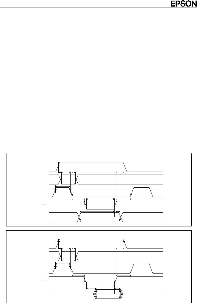
1. When ALE is used
Write mode |
|
( VDD=5 V ± 0.5 V, |
RTC-72421;Ta=− 10 ° C to +70 ° C, RTC-72423;Ta=− 40 ° C to +85 ° C ) |
|||||||||
Item |
|
|
|
Symbol |
Condition |
|
|
Min. |
Max. |
Unit |
|
|
|
|
|
|
|
|
|
|
|
|
|
|
|
CS1 set-up time |
|
|
|
tSU(CS1) |
|
|
|
1000 |
|
|
|
|
|
|
|
|
|
|
|
|
|
|
|
|
|
Address set-up time before ALE |
|
|
|
tSU(A-ALE) |
|
|
|
50 |
|
|
|
|
|
|
|
|
|
|
|
|
|
|
|
|
|
Address hold time after ALE |
|
|
|
th(ALE-A) |
|
|
|
50 |
|
|
|
|
ALE pulse width |
|
|
|
tw(ALE) |
|
|
|
80 |
|
|
|
|
ALE set-up time before write |
|
|
|
tSU(ALE-W) |
|
|
|
0 |
|
|
|
|
|
|
|
|
|
|
|
|
|
|
|
|
|
Write pulse width |
|
|
|
tw(W) |
|
|
|
120 |
|
ns |
|
|
|
|
|
|
|
|
|
|
|
|
|
|
|
ALE set-up time after write |
|
|
|
tSU(W-ALE) |
|
|
|
50 |
|
|
|
|
Data input set-up time before write |
|
|
|
tSU(D-W) |
|
|
|
80 |
|
|
|
|
|
|
|
|
|
|
|
|
|
|
|
|
|
Data input hold time after write |
|
|
|
th(W-D) |
|
|
|
10 |
|
|
|
|
|
|
|
|
|
|
|
|
|
|
|
|
|
CS1 hold time |
|
|
|
th(CS1) |
|
|
|
1000 |
|
|
|
|
|
|
|
|
|
|
|
|
|
|
|
|
|
Write recovery time |
|
|
|
trec(W) |
|
|
|
200 |
|
|
|
|
Read mode |
|
( VDD=5 V ± 0.5 V, |
RTC-72421;Ta=− 10 ° C to +70 ° C, RTC-72423;Ta=− 40 ° C to +85 ° C ) |
|||||||||
Item |
|
|
|
Symbol |
Condition |
|
|
Min. |
Max. |
Unit |
|
|
|
|
|
|
|
|
|
|
|
|
|
|
|
CS1 set-up time |
|
|
|
tSU(CS1) |
|
|
|
1000 |
|
|
|
|
|
|
|
|
|
|
|
|
|
|
|
|
|
Address set-up time before ALE |
|
|
|
tSU(A-ALE) |
|
|
|
50 |
|
|
|
|
Address hold time after ALE |
|
|
|
th(ALE-A) |
|
|
|
50 |
|
|
|
|
|
|
|
|
|
|
|
|
|
|
|
|
|
ALE pulse width |
|
|
|
tw(ALE) |
|
|
|
80 |
|
|
|
|
|
|
|
|
|
|
|
|
|
|
|
|
|
ALE set-up time before read |
|
|
|
tSU(ALE-R) |
|
|
|
0 |
|
ns |
|
|
ALE set-up time after read |
|
|
|
tSU(R-ALE) |
|
|
|
50 |
|
|
|
|
Data output transfer time after read |
|
|
|
tPZV(R-Q) |
CL=150 pF |
|
|
|
120 |
|
|
|
|
|
|
|
|
|
|
|
|
|
|
|
|
Data output floating transfer time after read |
|
tPVZ(R-Q) |
|
|
|
0 |
70 |
|
|
|||
|
|
|
|
|
|
|
|
|
|
|
|
|
CS1 hold time |
|
|
|
th(CS1) |
|
|
|
1000 |
|
|
|
|
Read recovery time |
|
|
|
trec(W) |
|
|
|
200 |
|
|
|
|
|
|
|
|
|
|
|
|
|
|
|
|
|
|
|
|
|
|
|
|
|
|
|
|
|
|
(1) Write mode |
|
|
|
|
|
|
|
|
|
|
|
|
|
|
|
VIH2 |
|
|
|
|
VIH2 |
|
|
|
|
CS1 |
|
|
|
|
|
|
|
|
|
|
|
|
|
|
tsu(CS1) |
|
|
|
|
|
|
|
|
|
|
|
|
|
tsu(A-ALE) |
th(ALE-A) |
th(CS1) |
|
|
|
|
|
|
|
|
|
|
|
|
|
|
|
|
|
|||
A0 to A3 |
VIH1 |
VIH1 |
|
|
|
|
|
||
|
|
|
|
|
CS0 |
VIL1 |
VIL1 |
|
|
|
tw(ALE) |
|
|
|
VIH1 |
VIH1 |
|
|
|
ALE |
|
|
|
|
|
|
VIL1 |
|
VIL1 |
|
|
tsu(ALE-W) |
tw(W) |
tsu(W-ALE) |
|
|
VIH1 |
|
VIH1 |
WR |
|
VIL1 |
|
VIL1 |
|
|
|
||
|
|
|
tsu(D-W) |
th(W-D) |
|
|
|
|
|
|
|
VIH1 |
|
VIH1 |
D0 to D3 |
|
|
|
|
(Input) |
|
VIL1 |
|
VIL1 |
(2) Read mode
|
VIH2 |
|
VIH2 |
CS1 |
|
|
|
|
|
|
|
tsu(CS1) |
|
th(CS1) |
|
|
tsu(A-ALE) th(ALE-A) |
||
|
|
||
A0 to A3 |
VIH1 |
VIH1 |
|
|
|
||
|
|
|
|
CS0 |
VIL1 |
VIL1 |
|
|
|
|
|
|
tw(ALE) |
|
|
VIH1 |
VIH1 |
|
|
ALE |
|
|
|
|
|
VIL1 |
VIL1 |
|
tsu(ALE-R) |
tsu(R-ALE) |
|
VIH1 |
VIH1 |
RD |
VIL1 |
VIL1 |
|
||
|
tpzv(R-Q) |
tpvz(R-Q) |
|
|
|
|
VIH1 |
VIH1 |
D0 to D3 |
|
|
(Input) |
VIL1 |
VIL1 |
Page - 5 |
MQ - 162 - 03 |
 Loading...