


 Loading...
KAT4000: AMC Carrier for ATCA®
User’s Manual
from Emerson Network Power™ Embedded Computing
April 2007
The information in this manual has been checked and is believed to be accurate and reliable. HOWEVER, NO RESPONSIBILITY IS ASSUMED BY ARTESYN COMMUNICATION PRODUCTS FOR ITS USE OR FOR ANY INACCURACIES. Specifications are subject to change without notice. ARTESYN COMMUNICATION PRODUCTS DOES NOT ASSUME ANY LIABILITY ARISING OUT OF USE OR OTHER APPLICATION OF ANY PRODUCT, CIRCUIT, OR PROGRAM DESCRIBED HEREIN. This document does not convey any license under Artesyn Communication Products patents or the rights of others.
Artesyn and the Artesyn logo are registered trademarks of Artesyn Technologies and are used by Artesyn Communication Products under license from Artesyn Technologies. All other trademarks are property of their respective owners.
Revision Level: |
Principal Changes: |
Date: |
10007175-00 |
Original release |
January 2007 |
|
|
|
10007175-01 |
Added “Appendix A” |
February 2007 |
|
|
|
10007175-02 |
Added PCIe functionality; Released 10 GbE-1 GbE |
April 2007 |
|
fat pipe switch |
|
|
|
|
Copyright © 2007 Artesyn Communication Products. All rights reserved.
Emerson. Consider It Solved is a trademark, and Business-Critical Continuity, Emerson Network Power, and the Emerson Network Power logo are trademarks and service marks of Emerson Electric Co. © 2007 Emerson Electric Co.


 Regulatory Agency Warnings & Notices


The Emerson KAT4000 meets the requirements set forth by the Federal Communications Commission (FCC) in Title 47 of the Code of Federal Regulations. The following information is provided as required by this agency.
This device complies with part 15 of the FCC Rules. Operation is subject to the following two conditions: (1) This device may not cause harmful interference, and (2) this device must accept any interference received, including interference that may cause undesired operation.
Caution:
!
FCC RULES AND REGULATIONS — PART 15
This equipment has been tested and found to comply with the limits for a Class B digital device, pursuant to part 15 of the FCC Rules. These limits are designed to provide reasonable protection against harmful interference in a residential installation. This equipment generates, uses and can radiate radio frequency energy and, if not installed and used in accordance with the instructions, may cause harmful interference to radio communications. However, there is no guarantee that interference will not occur in a particular installation. If this equipment does cause harmful interference to radio or television reception, which can be determined by turning the equipment off and on, the user is encouraged to try to correct the interference by one or more of the following measures:
•Reorient or relocate the receiving antenna
•Increase the separation between the equipment and receiver
•Connect the equipment into an outlet on a circuit different from that to which the receiver is connected
•Consult the dealer or an experienced radio/TV technician for help
Making changes or modifications to the KAT4000 hardware without the explicit consent of Emerson Network Power could invalidate the user’s authority to operate this equipment.
Caution:
!
EMC COMPLIANCE
The electromagnetic compatibility (EMC) tests used a KAT4000 model that includes a front panel assembly from Emerson Network Power.
For applications where the KAT4000 is provided without a front panel, or where the front panel has been removed, your system chassis/enclosure must provide the required electromagnetic interference (EMI) shielding to maintain CE compliance.
10007175-02 |
KAT4000 User’s Manual |
i |
|
|
|


 Regulatory Agency Warnings & Notices
 (continued)


|
|
|
|
|
|
|
|
|
|
|
|
|
|
|
|
|
|
|
|
|
|
|
|
|
|
|
|
|
|
|
|
|
|
|
|
|
|
|
|
|
|
|
|
|
|
|
|
|
|
|
|
|
|
|
|
|
|
|
|
|
|
|
|
|
|
|
|
|
|
|
|
|
|
|
|
|
|
|
|
|
|
|
|
|
|
|
|
|
|
|
|
|
|
|
|
|
|
|
|
|
|
|
|
|
|
EC Declaration of Conformity |
|
|
|
|
|
|
|
|
|
|
|
|
|
|
|
|
|
|
|
|
|
|
|
|
|
|
|||||||||||||||||||||||||
|
|
|
|
|
|
|
|
|
|
|
|
|
|
|
|
|
|
|
|
|
|
|
|
|
|
|
|
|
|
|
|
According to EN 45014:1998 |
|
|
|
|
|
|
|
|
|
|
|
|
|
|
|
|
|
|
|
|
|
|
|
|
|
|
||||||||||||||||||||
|
|
|
|
|
|
|
|
|
|
|
|
Manufacturer’s Name: |
|
|
|
Emerson Network Power |
|
|
|
|
|
|
|
|
|
|
|
|
|
|
|
|
|
|
|
|
|
|
|
|
|
|
||||||||||||||||||||||||||||||||||||
|
|
|
|
|
|
|
|
|
|
|
|
|
|
|
|
|
|
|
|
|
|
|
|
|
|
|
|
|
|
Embedded Computing |
|
|
|
|
|
|
|
|
|
|
|
|
|
|
|
|
|
|
|
|
|
|
|
|
|
|
||||||||||||||||||||||
|
|
|
|
|
|
|
|
|
|
|
|
Manufacturer’s Address: |
|
|
|
8310 Excelsior Drive |
|
|
|
|
|
|
|
|
|
|
|
|
|
|
|
|
|
|
|
|
|
|
|
|
|
|
||||||||||||||||||||||||||||||||||||
|
|
|
|
|
|
|
|
|
|
|
|
|
|
|
|
|
|
|
|
|
|
|
|
|
|
|
|
|
|
Madison, Wisconsin 53717 |
|
|
|
|
|
|
|
|
|
|
|
|
|
|
|
|
|
|
|
|
|
|
|
|
|
|
||||||||||||||||||||||
Declares that the following product, in accordance with the requirements of 89/336/EEC, EMC
Directive and 99/5/EC, RTTE Directive and their amending directives,
Product: |
ATCA Carrier |
Model Name/Number: |
KAT4000/10007505-xx |
has been designed and manufactured to the following specifications:
EN55022:1998 Information Technology Equipment, Radio disturbance characteristics, Limits and methods of measurement
EN55024:1998 Information Technology Equipment, Immunity characteristics, Limits and methods of measurement
EN300386 V.1.3.1 Electromagnetic compatibility and radio spectrum matters (ERM);
Telecommunication network equipment; EMC requirements
As manufacturer we hereby declare that the product named above has been designed to comply with the relevant sections of the above referenced specifications. This product complies with the essential health and safety requirements of the EMC Directive and RTTE Directive. We have an internal production control system that ensures compliance between the manufactured products and the technical documentation.
Bill Fleury
Compliance Engineer
Issue date: April 3, 2007
ii |
KAT4000 User’s Manual |
10007175-02 |
|
|
|


 Contents


1 Overview
Components and Features . . . . . . . . . . . 1-1
KAT4000 Options. . . . . . . . . . . . . . . . 1-3
Functional Overview . . . . . . . . . . . . . . . . 1-5
Physical Memory Map . . . . . . . . . . . . . . . 1-6
AMC Mapping . . . . . . . . . . . . . . . . . . . . . . 1-9
Additional Information . . . . . . . . . . . . . 1-10
Product Certification . . . . . . . . . . . .1-10
UL Certification. . . . . . . . . . . . . . . . .1-11
RoHS Compliance. . . . . . . . . . . . . . .1-11
Terminology and Notation . . . . . . .1-12
Technical References. . . . . . . . . . . .1-12
2 Setup
Electrostatic Discharge . . . . . . . . . . . . . . 2-1
KAT4000 Circuit Board . . . . . . . . . . . . . . 2-1
Front Panel . . . . . . . . . . . . . . . . . . . . . 2-4
Connectors . . . . . . . . . . . . . . . . . . . . . 2-4
Header JP4 . . . . . . . . . . . . . . . . . . . . . . 2-5
Jumpers . . . . . . . . . . . . . . . . . . . . . . . . 2-5
JTAG Interfaces . . . . . . . . . . . . . . . . . . 2-9
LEDs . . . . . . . . . . . . . . . . . . . . . . . . . .2-10
Reset. . . . . . . . . . . . . . . . . . . . . . . . . .2-13
KAT4000 Setup . . . . . . . . . . . . . . . . . . . . 2-15
Identification Numbers . . . . . . . . . .2-15
Power Requirements . . . . . . . . . . . .2-16
Environmental Considerations . . .2-16
Troubleshooting . . . . . . . . . . . . . . . . . . . 2-17
Technical Support . . . . . . . . . . . . . .2-17
Product Repair . . . . . . . . . . . . . . . . .2-18
3 Central Processing Unit
MPC8548 Functions . . . . . . . . . . . . . . . . . 3-3 Microprocessor Core (e500). . . . . . . . . . 3-3 L1 Cache. . . . . . . . . . . . . . . . . . . . . . . . 3-3
L2 Cache. . . . . . . . . . . . . . . . . . . . . . . . 3-3 Timer/Counter . . . . . . . . . . . . . . . . . . 3-4
PCI Device and Vendor ID Assignment. 3-4
L2 Control Register (L2CR) . . . . . . . . 3-4
Hardware Implementation Dependent 0 Register. . . . . . . . . . . . . . . . . . . . . . . 3-6 Hardware Implementation Dependent 1 Register. . . . . . . . . . . . . . . . . . . . . . . 3-7
Interrupts and Exception Processing. . . 3-8
Machine State Register. . . . . . . . . . . 3-9 Peripheral Interface . . . . . . . . . . . . . . . . 3-10 MPC8548 Peripheral Modules . . . . . . . 3-11
Three-Speed Ethernet Controllers (TSEC) . . . . . . . . . . . . . . . . . . . . . . . . 3-11 Local Bus Controller (LBC) . . . . . . . 3-12 Chip Select Generation. . . . . . . . . . 3-12
Processor Reset and Clocking Signals. 3-12 MPC8548 Exception Handling . . . . . . . 3-13 JTAG/COP Interface . . . . . . . . . . . . . . . . 3-14 No Processor Configuration . . . . . . . . . 3-15
4 Common Switch Region
Ethernet Core Switch (optional) . . . . . . .4-2 Switch Configuration . . . . . . . . . . . . 4-3 High-Speed Serial Data Path Configuration . . . . . . . . . . . . . . . . . . . 4-3
On-Board Path Device Settings 4-4
Off-Board Path Device Settings 4-4 Ethernet Transceivers . . . . . . . . . . . . 4-5
Ethernet Address for the KAT4000 . . . . .4-5 Ethernet Address for the GbE Fat Pipe Switch Module . . . . . . . . . . . . . . . . . . . . . . . . . . . . .4-6 PCI Express Switch (optional). . . . . . . . . .4-7 PCI Express Interface. . . . . . . . . . . . . 4-8 EEPROM Interface . . . . . . . . . . . . . . . 4-9 JTAG Controller Interface . . . . . . . . . 4-9
5 Fat Pipe Switch Module
GbE Fat Pipe Switch Module. . . . . . . . . . .5-2
GbE Fat Pipe Switch Module Circuit
Board . . . . . . . . . . . . . . . . . . . . . . . . . . 5-4
Components and Features. . . . . . . . 5-5
GbE Fat Pipe Switch Module PLD . . 5-6
Product ID/Version Register . . 5-6
Scratch Register . . . . . . . . . . . . . 5-7
I2C Register. . . . . . . . . . . . . . . . . 5-7
Signal Detect Register . . . . . . . 5-8
Switch Reset Register . . . . . . . . 5-8
Module Status Register . . . . . . 5-8
Switch GPIO Register . . . . . . . . 5-9
GPIN/LED Register . . . . . . . . . . . 5-9
10GbE-1 GbE Fat Pipe Switch Module 5-11 10 GbE-1 GbE Fat Pipe Switch Module
Circuit Board. . . . . . . . . . . . . . . . . . . 5-13
Components and Features. . . . . . . 5-14
10007175-02 |
KAT4000 User’s Manual |
iii |
|
|
|


 Contents
 (continued)


10 GbE-1 GbE Fat Pipe Switch Module
PLD . . . . . . . . . . . . . . . . . . . . . . . . . . .5-16
Product ID/Version Register. .5-16
Scratch Register . . . . . . . . . . . .5-17
I2C Register . . . . . . . . . . . . . . . .5-17
Reserved Register 1 . . . . . . . . .5-18
Switch Reset Register . . . . . . .5-18
Module Status Register . . . . . .5-19
Switch GPIO Register. . . . . . . .5-19
GPIN/LED Register . . . . . . . . . .5-20
10 GbE-10 GbE Fat Pipe Switch Module5-21
sRIO Fat Pipe Switch Module . . . . . . . . 5-22
6 Memory Configuration
Boot Memory Configuration . . . . . . . . . .6-1
User Flash. . . . . . . . . . . . . . . . . . . . . . . . . . .6-1
On-Card SDRAM . . . . . . . . . . . . . . . . . . . . .6-2
NAND Flash . . . . . . . . . . . . . . . . . . . . . . . . .6-2
NVRAM Allocation . . . . . . . . . . . . . . . . . . .6-3
7 CPLD
PLD Register Summary . . . . . . . . . . . . . . .7-1 Version and ID Registers . . . . . . . . . . . . . .7-2 Product ID Register (PIDR) . . . . . . . . 7-2
Hardware Version Register (HVR) . . 7-3 PLD Version Register (PVR) . . . . . . . 7-3
Configuration Registers . . . . . . . . . . . . . .7-4
Hardware Configuration Register 0 (HCR0) . . . . . . . . . . . . . . . . . . . . . . . . . 7-4
PLL Configuration Register (PLLC). . 7-4 Miscellaneous Registers . . . . . . . . . . . . . .7-5 LED Control Register (LEDR). . . . . . . 7-5 Jumper Settings Register (JSR). . . . . 7-6 RTM GPIO State Register (RGSR). . . 7-6 RTM GPIO Control Register (RGCR) 7-7 MISC Control Register (MISC) . . . . . 7-7 Scratch Register 1 (SCR1) . . . . . . . . . 7-8 Boot and Reset Registers . . . . . . . . . . . . .7-8 Reset Event Register (RER) . . . . . . . . 7-8 Reset Command Register 1 (RCR1) 7-9 Reset Command Register 2 (RCR2)7-10
Boot Device Redirection Register (BDRR) . . . . . . . . . . . . . . . . . . . . . . . .7-11
Clock Synchronizer Registers . . . . . . . . 7-13 Clock Synchronizer Control Registers 1- 3 (CSC1—CSC3) . . . . . . . . . . . . . . . . .7-13
Clock Synchronizer Primary Source Registers 1-3 (CPS1—CPS3) . . . . . . 7-14 Clock Synchronizer Secondary Source Registers 1-3 (CSS1—CSS3) . . . . . . 7-15
Clock Control Registers (CCR1—CCR14) 7-17
Clock Synchronizer Interrupt Registers (CSI1-CSI3) . . . . . . . . . . . . . . . . . . . . 7-18 JTAG Interface . . . . . . . . . . . . . . . . . . . . . 7-19
8 AMC Sites
AMC Connectors . . . . . . . . . . . . . . . . . . . .8-2
AMC Signals. . . . . . . . . . . . . . . . . . . . . . . . .8-2
Pin Assignments . . . . . . . . . . . . . . . . . . . . .8-4
SATA Lines . . . . . . . . . . . . . . . . . . . . . . . . . .8-6
9 System Management
IPMC Overview . . . . . . . . . . . . . . . . . . . . . .9-1 IPMI Messaging. . . . . . . . . . . . . . . . . . . . . .9-3 IPMI Completion Codes . . . . . . . . . . 9-4 IPMB Protocol . . . . . . . . . . . . . . . . . . . . . . .9-5 SIPL Protocol . . . . . . . . . . . . . . . . . . . . . . . .9-6 Message Bridging. . . . . . . . . . . . . . . . . . . .9-7 Standard Commands. . . . . . . . . . . . . . . . .9-9 Vendor Commands . . . . . . . . . . . . . . . . 9-12 Get Status Command . . . . . . . . . . . 9-12
Get Serial Interface Properties Command . . . . . . . . . . . . . . . . . . . . . 9-14 Set Serial Interface Properties Command . . . . . . . . . . . . . . . . . . . . . 9-15 Get Debug Level Command . . . . . 9-16 Set Debug Level Command . . . . . . 9-17 Get Hardware Address Command 9-17 Set Hardware Address Command 9-18 Get Handle Switch Command. . . . 9-18 Set Handle Switch Command . . . . 9-19
Get Payload Communication Time-Out Command . . . . . . . . . . . . . . . . . . . . . 9-19
Set Payload Communication Time-Out Command . . . . . . . . . . . . . . . . . . . . . 9-20 Enable Payload Control Command9-20
Disable Payload Control Command . . .
9-20
Reset IPMC Command . . . . . . . . . . 9-21 Hang IPMC Command . . . . . . . . . . 9-21 Bused Resource Control Command . . .
9-22
iv |
KAT4000 User’s Manual |
10007175-02 |
|
|
|


 Contents
 (continued)


Bused Resource Status Command 9-22 Graceful Reset Command. . . . . . . .9-23 Diagnostic Interrupt Results . . . . .9-24 Get Payload Shutdown Time-Out Command . . . . . . . . . . . . . . . . . . . . .9-24 Set Payload Shutdown Time-Out Command . . . . . . . . . . . . . . . . . . . . .9-25 Get Module State Command . . . . .9-25 Enable AMC Site Command . . . . . .9-26 Disable AMC Site Command . . . . .9-26
IPMC Watchdog Timer Commands. . . 9-27 Watchdog Timer Actions . . . . . . . .9-27
Watchdog Timer Use Field and Expiration Flags . . . . . . . . . . . . . . . .9-27
Using the Timer Use Field and Expiration Flags. . . . . . . . . . . . .9-28
Watchdog Timer Event Logging . .9-28
Monitor Support for Watchdog Timer . . . . . . . . . . . . . . . . . . . . .9-29
Reset Watchdog Timer Command9-29 Set Watchdog Timer Command . .9-29 Get Watchdog Timer Command. .9-31 FRU LEDs . . . . . . . . . . . . . . . . . . . . . . . . . 9-33 Get FRU LED Properties Command9-34 Get LED Color Capabilities Command .
9-34
Set FRU LED State Command. . . . .9-36 Get FRU LED State Command . . . .9-38
Entities and Entity Associations . . . . . . 9-39 Sensors and Sensor Data Records . . . . 9-40 FRU Inventory . . . . . . . . . . . . . . . . . . . . . 9-44 E-Keying . . . . . . . . . . . . . . . . . . . . . . . . . . 9-45 Base Point-to-Point Connectivity .9-45
Carrier Point-to-Point Connectivity9-46 Firmware Upgrade . . . . . . . . . . . . . . . . . 9-47 Firmware Upgrade Status Command. .
9-47
Firmware Upgrade Start Command . . .
9-48
Firmware Upgrade Prepare Command 9-49
Firmware Upgrade Write Command . . 9-49
Firmware Upgrade Complete Command . . . . . . . . . . . . . . . . . . . . .9-50
Firmware Upgrade Restore Backup Command . . . . . . . . . . . . . . . . . . . . .9-50
Firmware Upgrade Backup Revision Command . . . . . . . . . . . . . . . . . . . . .9-51
Firmware Upgrade Termination . . 9-51
Firmware Upgrade Sequence . . . . 9-51
10Synchronization Clocks
MT9045 and MT9046 Clock Synchronizers . 10-2
11Real-Time Clock
Block Diagram. . . . . . . . . . . . . . . . . . . . . 11-1 Operation . . . . . . . . . . . . . . . . . . . . . . . . 11-1 Clock Operation . . . . . . . . . . . . . . . . . . . 11-2
12Connectors
Zone 1 . . . . . . . . . . . . . . . . . . . . . . . . . . . 12-1 Zone 2 . . . . . . . . . . . . . . . . . . . . . . . . . . . 12-2 Zone 3 . . . . . . . . . . . . . . . . . . . . . . . . . . . 12-4
13Rear Transition Module
Components and Features . . . . . . . . . . 13-1 Functional Overview . . . . . . . . . . . . . . . 13-2 Circuit Board . . . . . . . . . . . . . . . . . . . . . . 13-3 Face Plate. . . . . . . . . . . . . . . . . . . . . . . . . 13-5 Connectors . . . . . . . . . . . . . . . . . . . . . . . 13-5
Console Serial Ports. . . . . . . . . . . . . 13-5 Ethernet Port . . . . . . . . . . . . . . . . . . 13-6 Zone 3 . . . . . . . . . . . . . . . . . . . . . . . . 13-6 Setup . . . . . . . . . . . . . . . . . . . . . . . . . . . . 13-6 Identification Numbers . . . . . . . . . 13-7 Installation. . . . . . . . . . . . . . . . . . . . . . . . 13-7
14Monitor
Command-Line Features. . . . . . . . . . . . 14-1 Basic Operation . . . . . . . . . . . . . . . . . . . 14-4 Power-up/Reset Sequence . . . . . . 14-4 POST Diagnostic Results . . . . . . . . 14-6 Monitor SDRAM Usage . . . . . . . . . . 14-6 Monitor Recovery and Updates . . . . . . 14-6 Recovering the Monitor . . . . . . . . . 14-7 Resetting Environment Variables . 14-7 Updating the Monitor via TFTP . . . 14-7 Monitor Command Reference . . . . . . . 14-8 Command Syntax . . . . . . . . . . . . . . 14-8 Command Help . . . . . . . . . . . . . . . . 14-9
10007175-02 |
KAT4000 User’s Manual |
v |
|
|
|


 Contents
 (continued)


Typographic Conventions . . . . . . .14-9
Boot Commands. . . . . . . . . . . . . . . . . . . 14-9 bootd . . . . . . . . . . . . . . . . . . . . . . . . .14-9
bootelf . . . . . . . . . . . . . . . . . . . . . . . .14-9 bootm . . . . . . . . . . . . . . . . . . . . . . . .14-9 bootp . . . . . . . . . . . . . . . . . . . . . . . . .14-9 bootv . . . . . . . . . . . . . . . . . . . . . . . .14-10 bootvx . . . . . . . . . . . . . . . . . . . . . . .14-10 dhcp . . . . . . . . . . . . . . . . . . . . . . . . .14-10 rarpboot. . . . . . . . . . . . . . . . . . . . . .14-11 tftpboot . . . . . . . . . . . . . . . . . . . . . .14-11
File Load Commands . . . . . . . . . . . . . . 14-12 loadb . . . . . . . . . . . . . . . . . . . . . . . .14-12 loads . . . . . . . . . . . . . . . . . . . . . . . . .14-12
Memory Commands . . . . . . . . . . . . . . 14-12 cmp. . . . . . . . . . . . . . . . . . . . . . . . . .14-13
cp . . . . . . . . . . . . . . . . . . . . . . . . . . .14-13 find . . . . . . . . . . . . . . . . . . . . . . . . . .14-13 md. . . . . . . . . . . . . . . . . . . . . . . . . . .14-13 mm . . . . . . . . . . . . . . . . . . . . . . . . . .14-14 nm. . . . . . . . . . . . . . . . . . . . . . . . . . .14-14 mw . . . . . . . . . . . . . . . . . . . . . . . . . .14-14
Flash Commands . . . . . . . . . . . . . . . . . 14-15 cp . . . . . . . . . . . . . . . . . . . . . . . . . . .14-15 erase . . . . . . . . . . . . . . . . . . . . . . . . .14-15 flinfo . . . . . . . . . . . . . . . . . . . . . . . . .14-15 protect . . . . . . . . . . . . . . . . . . . . . . .14-16
EEPROM/I2C Commands . . . . . . . . . . 14-16 eeprom . . . . . . . . . . . . . . . . . . . . . .14-16 icrc32 . . . . . . . . . . . . . . . . . . . . . . . .14-17 iloop . . . . . . . . . . . . . . . . . . . . . . . . .14-17 imd . . . . . . . . . . . . . . . . . . . . . . . . . .14-17 imd2 . . . . . . . . . . . . . . . . . . . . . . . . .14-17 imm . . . . . . . . . . . . . . . . . . . . . . . . .14-17 imm2 . . . . . . . . . . . . . . . . . . . . . . . .14-17 imw. . . . . . . . . . . . . . . . . . . . . . . . . .14-18 inm . . . . . . . . . . . . . . . . . . . . . . . . . .14-18 iprobe. . . . . . . . . . . . . . . . . . . . . . . .14-18 iprobe2. . . . . . . . . . . . . . . . . . . . . . .14-18 switchsrom . . . . . . . . . . . . . . . . . . .14-18
IPMC Commands . . . . . . . . . . . . . . . . . 14-18 fru . . . . . . . . . . . . . . . . . . . . . . . . . . .14-18
fruinit . . . . . . . . . . . . . . . . . . . . . . . .14-19 fruled . . . . . . . . . . . . . . . . . . . . . . . .14-19 ipmcfw . . . . . . . . . . . . . . . . . . . . . . .14-19 sensor. . . . . . . . . . . . . . . . . . . . . . . .14-19 Environment Parameter Commands 14-20
printenv. . . . . . . . . . . . . . . . . . . . . . 14-21 saveenv . . . . . . . . . . . . . . . . . . . . . . 14-21 setenv . . . . . . . . . . . . . . . . . . . . . . . 14-21
Test Commands . . . . . . . . . . . . . . . . . . 14-21 diags. . . . . . . . . . . . . . . . . . . . . . . . . 14-21
mtest . . . . . . . . . . . . . . . . . . . . . . . . 14-21 um . . . . . . . . . . . . . . . . . . . . . . . . . . 14-22
Other Commands. . . . . . . . . . . . . . . . . 14-22 autoscr. . . . . . . . . . . . . . . . . . . . . . . 14-22 base . . . . . . . . . . . . . . . . . . . . . . . . . 14-22 bdinfo . . . . . . . . . . . . . . . . . . . . . . . 14-22 coninfo . . . . . . . . . . . . . . . . . . . . . . 14-22 crc32 . . . . . . . . . . . . . . . . . . . . . . . . 14-22 date . . . . . . . . . . . . . . . . . . . . . . . . . 14-22 echo . . . . . . . . . . . . . . . . . . . . . . . . . 14-23 enumpci . . . . . . . . . . . . . . . . . . . . . 14-23 go . . . . . . . . . . . . . . . . . . . . . . . . . . . 14-23 help . . . . . . . . . . . . . . . . . . . . . . . . . 14-23 iminfo . . . . . . . . . . . . . . . . . . . . . . . 14-23 isdram . . . . . . . . . . . . . . . . . . . . . . . 14-23 loop . . . . . . . . . . . . . . . . . . . . . . . . . 14-24 memmap . . . . . . . . . . . . . . . . . . . . 14-24 moninit . . . . . . . . . . . . . . . . . . . . . . 14-24 pci. . . . . . . . . . . . . . . . . . . . . . . . . . . 14-24 phy . . . . . . . . . . . . . . . . . . . . . . . . . . 14-25 ping . . . . . . . . . . . . . . . . . . . . . . . . . 14-25 reset . . . . . . . . . . . . . . . . . . . . . . . . . 14-25 run . . . . . . . . . . . . . . . . . . . . . . . . . . 14-26 script . . . . . . . . . . . . . . . . . . . . . . . . 14-26 showmac. . . . . . . . . . . . . . . . . . . . . 14-26 showpci . . . . . . . . . . . . . . . . . . . . . . 14-26 sleep. . . . . . . . . . . . . . . . . . . . . . . . . 14-26 switch_reg . . . . . . . . . . . . . . . . . . . 14-27 version . . . . . . . . . . . . . . . . . . . . . . . 14-27 vlan. . . . . . . . . . . . . . . . . . . . . . . . . . 14-27
Environment Variables . . . . . . . . . . . . 14-28 Troubleshooting. . . . . . . . . . . . . . . . . . 14-31 Download Formats. . . . . . . . . . . . . . . . 14-32 Binary. . . . . . . . . . . . . . . . . . . . . . . . 14-32 Motorola S-Record . . . . . . . . . . . . 14-32
15Acronym List
16Appendix A
No-CPU KAT4000 . . . . . . . . . . . . . . . . . . . .A-1
vi |
KAT4000 User’s Manual |
10007175-02 |
|
|
|


 Contents
 (continued)


Ethernet Switch Configuration . . . . . . . A-2
Default Switch Configuration . . . . . A-2
Serial Command Line Interface (CLI). . . A-3
Log In/Log Out Procedures. . . . . . . . A-3
Help Utility. . . . . . . . . . . . . . . . . . . . . .A-3
Command Hierarchy . . . . . . . . . . . . . A-4
Command Usage Instructions . . . . .A-5
Commands . . . . . . . . . . . . . . . . . . . . . A-5
Command Overview . . . . . . . . . A-6
System Commands . . . . . . . . . . A-8
Console Commands . . . . . . . . . A-8
Port Commands . . . . . . . . . . . . .A-9
MAC Commands . . . . . . . . . . .A-10
VLAN Commands . . . . . . . . . . A-12
Aggregation/Trunking Commands
A-13
User Group Commands . . . . . A-14
QoS Commands. . . . . . . . . . . . A-14
Mirror Commands . . . . . . . . . . A-16
IP Commands . . . . . . . . . . . . . . A-16
Debug Commands . . . . . . . . . A-17
Web Interface . . . . . . . . . . . . . . . . . . . . . A-18
17Appendix B
Sensor Data Records . . . . . . . . . . . . . . . . .B-1
10007175-02 |
KAT4000 User’s Manual |
vii |
|
|
|

(blank page)
viii |
KAT4000 User’s Manual |
10007175-02 |
|
|
|


 Figures


Figure 1-1: General System Block Diagram. . . . . . . . . . . . . . . . . . . . . . . . . . . . . . . . . . . . . . . . . . . . . . 1-5 Figure 1-2: KAT4000 Memory Map. . . . . . . . . . . . . . . . . . . . . . . . . . . . . . . . . . . . . . . . . . . . . . . . . . . . . 1-6 Figure 1-3: AMC Port Mapping Regions. . . . . . . . . . . . . . . . . . . . . . . . . . . . . . . . . . . . . . . . . . . . . . . . . 1-9 Figure 2-1: Component Map, Top (Rev. 02) . . . . . . . . . . . . . . . . . . . . . . . . . . . . . . . . . . . . . . . . . . . . . 2-2 Figure 2-2: Component Map, Bottom (Rev. 02). . . . . . . . . . . . . . . . . . . . . . . . . . . . . . . . . . . . . . . . . . 2-3 Figure 2-3: KAT4000 Front Panel . . . . . . . . . . . . . . . . . . . . . . . . . . . . . . . . . . . . . . . . . . . . . . . . . . . . . . 2-4 Figure 2-4: Jumper, Fuse and Switch Locations, Top. . . . . . . . . . . . . . . . . . . . . . . . . . . . . . . . . . . . . . 2-7 Figure 2-5: Jumper, Fuse and Switch Locations, Bottom . . . . . . . . . . . . . . . . . . . . . . . . . . . . . . . . . . 2-8 Figure 2-6: JTAG Hubs . . . . . . . . . . . . . . . . . . . . . . . . . . . . . . . . . . . . . . . . . . . . . . . . . . . . . . . . . . . . . . . . 2-9 Figure 2-7: LEDs, Top. . . . . . . . . . . . . . . . . . . . . . . . . . . . . . . . . . . . . . . . . . . . . . . . . . . . . . . . . . . . . . . . 2-11 Figure 2-8: LEDs, Bottom . . . . . . . . . . . . . . . . . . . . . . . . . . . . . . . . . . . . . . . . . . . . . . . . . . . . . . . . . . . . 2-12 Figure 2-9: KAT4000 Reset Diagram . . . . . . . . . . . . . . . . . . . . . . . . . . . . . . . . . . . . . . . . . . . . . . . . . . 2-14 Figure 3-1: MPC8548 Block Diagram . . . . . . . . . . . . . . . . . . . . . . . . . . . . . . . . . . . . . . . . . . . . . . . . . . . 3-2 Figure 3-2: Processor JTAG/COP Diagram . . . . . . . . . . . . . . . . . . . . . . . . . . . . . . . . . . . . . . . . . . . . . . 3-14 Figure 3-3: Processor JTAG/COP Header . . . . . . . . . . . . . . . . . . . . . . . . . . . . . . . . . . . . . . . . . . . . . . . 3-14 Figure 4-1: Board Area Network . . . . . . . . . . . . . . . . . . . . . . . . . . . . . . . . . . . . . . . . . . . . . . . . . . . . . . . 4-1 Figure 4-2: VSC7376 GbE Switch Block Diagram . . . . . . . . . . . . . . . . . . . . . . . . . . . . . . . . . . . . . . . . . 4-3 Figure 4-3: PEX 8524 Block Diagram . . . . . . . . . . . . . . . . . . . . . . . . . . . . . . . . . . . . . . . . . . . . . . . . . . . 4-8 Figure 4-4: PEX 8524 SPI EEPROM Interface . . . . . . . . . . . . . . . . . . . . . . . . . . . . . . . . . . . . . . . . . . . . . 4-9 Figure 5-1: AMC Port Map Fat Pipes Region–GbE . . . . . . . . . . . . . . . . . . . . . . . . . . . . . . . . . . . . . . . . 5-2 Figure 5-2: Signal Routing of the GbE Fat Pipe Switch Module on the KAT4000 . . . . . . . . . . . . . . 5-2 Figure 5-3: GbE Fat Pipe Switch Module Block Diagram . . . . . . . . . . . . . . . . . . . . . . . . . . . . . . . . . . . 5-3 Figure 5-4: GbE Fat Pipe Switch Module Component Map, Top (Rev. 00). . . . . . . . . . . . . . . . . . . . 5-4 Figure 5-5: GbE Fat Pipe Switch Module Component Map, Bottom (Rev. 00) . . . . . . . . . . . . . . . . 5-4 Figure 5-6: GbE Fat Pipe Switch JTAG . . . . . . . . . . . . . . . . . . . . . . . . . . . . . . . . . . . . . . . . . . . . . . . . . . . 5-5 Figure 5-7: GbE Fat Pipe Switch Reset . . . . . . . . . . . . . . . . . . . . . . . . . . . . . . . . . . . . . . . . . . . . . . . . . . 5-6 Figure 5-8: AMC Port Map Fat Pipes Region–10 GbE-1 GbE . . . . . . . . . . . . . . . . . . . . . . . . . . . . . . 5-11 Figure 5-9: Signal Routing of the 10 GbE-1 GbE Fat Pipe Switch Module on the KAT4000 . . . . 5-11 Figure 5-10: 10 GbE-1 GbE Fat Pipe Switch Module Block Diagram . . . . . . . . . . . . . . . . . . . . . . . . . 5-12 Figure 5-11: 10 GbE-1 GbE Fat Pipe Switch Module Component Map, Top (Rev. 01) . . . . . . . . . . 5-13 Figure 5-12: 10 GbE-1 GbE Fat Pipe Switch Module Component Map, Bottom (Rev. 01) . . . . . . 5-13 Figure 5-13: 10 GbE-1 GbE Fat Pipe Switch JTAG . . . . . . . . . . . . . . . . . . . . . . . . . . . . . . . . . . . . . . . . . 5-15 Figure 5-14: 10 GbE-1 GbE Fat Pipe Switch Reset . . . . . . . . . . . . . . . . . . . . . . . . . . . . . . . . . . . . . . . . 5-16 Figure 5-15: AMC Port Map Fat Pipes Region–10 GbE-10 GbE . . . . . . . . . . . . . . . . . . . . . . . . . . . . . 5-21 Figure 5-16: Signal Routing of the 10 GbE-10 GbE Fat Pipe Switch Module on the KAT4000 . . . 5-21 Figure 5-17: AMC Port Map Fat Pipes Region–sRIO . . . . . . . . . . . . . . . . . . . . . . . . . . . . . . . . . . . . . . 5-22 Figure 5-18: Signal Routing of the sRIO Fat Pipe Switch Module on the KAT4000. . . . . . . . . . . . . 5-22 Figure 7-1: Boot Device Redirection. . . . . . . . . . . . . . . . . . . . . . . . . . . . . . . . . . . . . . . . . . . . . . . . . . . 7-12 Figure 7-2: PLD JTAG Diagram . . . . . . . . . . . . . . . . . . . . . . . . . . . . . . . . . . . . . . . . . . . . . . . . . . . . . . . . 7-20 Figure 8-1: AMC B+ Connector . . . . . . . . . . . . . . . . . . . . . . . . . . . . . . . . . . . . . . . . . . . . . . . . . . . . . . . . 8-2
10007175-02 |
KAT4000 User’s Manual |
ix |
|
|
|


 Figures
 (continued)


|
|
|
|
|
|
|
|
|
|
|
|
|
|
|
|
|
|
|
|
|
|
|
|
|
|
|
|
|
|
|
|
|
|
|
|
|
|
|
|
|
|
|
|
|
|
|
|
|
|
|
|
|
|
|
|
|
|
|
|
|
|
|
|
|
|
|
|
|
|
|
|
|
|
|
|
|
|
|
|
|
|
|
|
|
|
|
|
|
|
|
|
|
|
|
|
|
|
|
Figure 8-2: |
. . . . . . . . . . . . . . . . . . . . . . . . . . . . . . . . . . . . . . . . . . .Diagram of SATA line connections |
8-6 |
|
|
|
|
|
|
||||||||||||||||||||||||||||||||||||||||||||||||||
|
|
|
|
|
|
|
|
|
|
|
|
|
|
|
|
|
|
|
|
Figure 9-1: |
IPMC Connections Block Diagram . . . . . . . . . . . . . . . . . . . . . . . . . . . . . . . . . . . . . . . . . . . |
9-2 |
|
|
|
|
|
|
||||||||||||||||||||||||||||||||||||||||||||||||||
|
|
|
|
|
|
|
|
|
|
|
|
|
|
|
|
|
|
|
|
Figure 9-2: |
Extension Command Request Example. . . . . . . . . . . . . . . . . . . . . . . . . . . . . . . . . . . . . . . |
9-7 |
|
|
|
|
|
|
||||||||||||||||||||||||||||||||||||||||||||||||||
|
|
|
|
|
|
|
|
|
|
|
|
|
|
|
|
|
|
|
|
Figure 9-3: |
Extension Command Response Example . . . . . . . . . . . . . . . . . . . . . . . . . . . . . . . . . . . . . |
9-7 |
|
|
|
|
|
|
||||||||||||||||||||||||||||||||||||||||||||||||||
|
|
|
|
|
|
|
|
|
|
|
|
|
|
|
|
|
|
|
|
Figure 9-4: |
IPMB Entity Structure . . . . . . . . . . . . . . . . . . . . . . . . . . . . . . . . . . . . . . . . . . . . . . . . . . . . . |
9-40 |
|
|
|
|
|
|
||||||||||||||||||||||||||||||||||||||||||||||||||
|
|
|
|
|
|
|
|
|
|
|
|
|
|
|
|
|
|
|
|
Figure 10-1: |
Synchronization Clock Circuit Diagram. . . . . . . . . . . . . . . . . . . . . . . . . . . . . . . . . . . . . . |
10-1 |
|
|
|
|
|
|
||||||||||||||||||||||||||||||||||||||||||||||||||
|
|
|
|
|
|
|
|
|
|
|
|
|
|
|
|
|
|
|
|
Figure 11-1: |
M41T00 Real-Time Clock Block Diagram . . . . . . . . . . . . . . . . . . . . . . . . . . . . . . . . . . . . |
11-1 |
|
|
|
|
|
|
||||||||||||||||||||||||||||||||||||||||||||||||||
|
|
|
|
|
|
|
|
|
|
|
|
|
|
|
|
|
|
|
|
Figure 12-1: |
Zone 1 Connector, P10. . . . . . . . . . . . . . . . . . . . . . . . . . . . . . . . . . . . . . . . . . . . . . . . . . . . |
12-1 |
|
|
|
|
|
|
||||||||||||||||||||||||||||||||||||||||||||||||||
|
|
|
|
|
|
|
|
|
|
|
|
|
|
|
|
|
|
|
|
Figure 12-2: |
Zone 2 Connectors, J20 and J23, and Zone 3 Connectors, J30-J32. . . . . . . . . . . . . . . |
12-3 |
|
|
|
|
|
|
||||||||||||||||||||||||||||||||||||||||||||||||||
|
|
|
|
|
|
|
|
|
|
|
|
|
|
|
|
|
|
|
|
Figure 12-3: |
Zone 3 Connector, J33 . . . . . . . . . . . . . . . . . . . . . . . . . . . . . . . . . . . . . . . . . . . . . . . . . . . . |
12-7 |
|
|
|
|
|
|
||||||||||||||||||||||||||||||||||||||||||||||||||
|
|
|
|
|
|
|
|
|
|
|
|
|
|
|
|
|
|
|
|
Figure 13-1: |
RTM General System Block Diagram with Face Plate . . . . . . . . . . . . . . . . . . . . . . . . . . |
13-2 |
|
|
|
|
|
|
||||||||||||||||||||||||||||||||||||||||||||||||||
|
|
|
|
|
|
|
|
|
|
|
|
|
|
|
|
|
|
|
|
Figure 13-2: |
RTM Component Map, Top (Rev. 00) . . . . . . . . . . . . . . . . . . . . . . . . . . . . . . . . . . . . . . . |
13-4 |
|
|
|
|
|
|
||||||||||||||||||||||||||||||||||||||||||||||||||
|
|
|
|
|
|
|
|
|
|
|
|
|
|
|
|
|
|
|
|
Figure 13-3: |
Micro-D Console Cable . . . . . . . . . . . . . . . . . . . . . . . . . . . . . . . . . . . . . . . . . . . . . . . . . . . . |
13-5 |
|
|
|
|
|
|
||||||||||||||||||||||||||||||||||||||||||||||||||
|
|
|
|
|
|
|
|
|
|
|
|
|
|
|
|
|
|
|
|
Figure 13-4: |
Standard Console Cable Wiring, #10007665-xx . . . . . . . . . . . . . . . . . . . . . . . . . . . . . . |
13-6 |
|
|
|
|
|
|
||||||||||||||||||||||||||||||||||||||||||||||||||
|
|
|
|
|
|
|
|
|
|
|
|
|
|
|
|
|
|
|
|
Figure 13-5: |
Installing a KAT-Z3DB RTM on the KAT4000 . . . . . . . . . . . . . . . . . . . . . . . . . . . . . . . . . |
13-8 |
|
|
|
|
|
|
||||||||||||||||||||||||||||||||||||||||||||||||||
|
|
|
|
|
|
|
|
|
|
|
|
|
|
|
|
|
|
|
|
Figure 14-1: |
Example Monitor Start-up Display for KAT4000 with GbE Fat Pipe Switch Module |
14-2 |
|
|
|
|
|
|
||||||||||||||||||||||||||||||||||||||||||||||||||
|
|
|
|
|
|
|
|
|
|
|
|
|
|
|
|
|
|
|
|
Figure 14-2: |
Example Monitor Start-up Display for KAT4000 with 10 GbE-1 GbE Fat Pipe Switch Mod- |
|
|
|
|
|
|
|||||||||||||||||||||||||||||||||||||||||||||||||||
|
|
|
|
|
|
|
|
|
|
|
|
|
|
|
|
|
|
|
|
ule |
|
. |
. . . |
. |
. . |
. . |
. . |
. |
. . |
. . |
. . |
. |
. . . |
. |
. . |
. |
. . . |
. |
. . |
. |
. . . |
. |
. . |
. . |
. . |
. |
. . . |
. |
. . |
. |
. . . |
. |
. . |
. |
. . . |
. |
. . |
. . |
. . |
. |
. . |
. |
14-3 |
|
|
|
|
|
|
|||||||||
|
|
|
|
|
|
|
|
|
|
|
|
|
|
|
|
|
|
|
|
Figure 14-3: |
Power-up/Reset Sequence Flowchart . . . . . . . . . . . . . . . . . . . . . . . . . . . . . . . . . . . . . . . |
14-5 |
|
|
|
|
|
|
||||||||||||||||||||||||||||||||||||||||||||||||||
|
|
|
|
|
|
|
|
|
|
|
|
|
|
|
|
|
|
|
|
Figure A-1: |
No-CPU KAT4000 System Block Diagram . . . . . . . . . . . . . . . . . . . . . . . . . . . . . . . . . . . . . |
A-1 |
|
|
|
|
|
|
||||||||||||||||||||||||||||||||||||||||||||||||||
|
|
|
|
|
|
|
|
|
|
|
|
|
|
|
|
|
|
|
|
Figure A-2: |
Web Interface for the Ethernet Core Switch. . . . . . . . . . . . . . . . . . . . . . . . . . . . . . . . . . |
A-20 |
|
|
|
|
|
|
||||||||||||||||||||||||||||||||||||||||||||||||||
x |
KAT4000 User’s Manual |
10007175-02 |
|
|
|


 Tables


Table 1-1: KAT4000 Address Summary . . . . . . . . . . . . . . . . . . . . . . . . . . . . . . . . . . . . . . . . . . . . . . . . 1-7 Table 1-2: Regulatory Agency Compliance . . . . . . . . . . . . . . . . . . . . . . . . . . . . . . . . . . . . . . . . . . . . 1-10 Table 1-3: Technical References . . . . . . . . . . . . . . . . . . . . . . . . . . . . . . . . . . . . . . . . . . . . . . . . . . . . . 1-12 Table 2-1: Circuit Board Dimensions . . . . . . . . . . . . . . . . . . . . . . . . . . . . . . . . . . . . . . . . . . . . . . . . . . 2-1 Table 2-2: JP4 Signal Descriptions . . . . . . . . . . . . . . . . . . . . . . . . . . . . . . . . . . . . . . . . . . . . . . . . . . . . . 2-5 Table 2-3: Jumpers–JP2 and JP7 . . . . . . . . . . . . . . . . . . . . . . . . . . . . . . . . . . . . . . . . . . . . . . . . . . . . . . 2-6 Table 2-4: J35 Signal Descriptions . . . . . . . . . . . . . . . . . . . . . . . . . . . . . . . . . . . . . . . . . . . . . . . . . . . . 2-10 Table 2-5: Typical Power Requirement. . . . . . . . . . . . . . . . . . . . . . . . . . . . . . . . . . . . . . . . . . . . . . . . 2-16 Table 2-6: Environmental Requirements . . . . . . . . . . . . . . . . . . . . . . . . . . . . . . . . . . . . . . . . . . . . . . 2-16 Table 2-7: Air Flow Requirements . . . . . . . . . . . . . . . . . . . . . . . . . . . . . . . . . . . . . . . . . . . . . . . . . . . . 2-16 Table 3-1: MPC8548 Features . . . . . . . . . . . . . . . . . . . . . . . . . . . . . . . . . . . . . . . . . . . . . . . . . . . . . . . . 3-1 Table 3-2: PCI Device and Vendor ID. . . . . . . . . . . . . . . . . . . . . . . . . . . . . . . . . . . . . . . . . . . . . . . . . . . 3-4 Table 3-3: MPC8548 Peripheral Request Priority . . . . . . . . . . . . . . . . . . . . . . . . . . . . . . . . . . . . . . . 3-10 Table 3-4: MPC8548 Chip Select . . . . . . . . . . . . . . . . . . . . . . . . . . . . . . . . . . . . . . . . . . . . . . . . . . . . . 3-12 Table 3-5: MPC8548 Exceptions . . . . . . . . . . . . . . . . . . . . . . . . . . . . . . . . . . . . . . . . . . . . . . . . . . . . . 3-13 Table 3-6: Processor JTAG/COP Pin Assignments (P1). . . . . . . . . . . . . . . . . . . . . . . . . . . . . . . . . . . 3-15 Table 4-1: KAT4000 PHYs and Address Values . . . . . . . . . . . . . . . . . . . . . . . . . . . . . . . . . . . . . . . . . . 4-4 Table 4-2: Ethernet Core Switch Off-Board Ports . . . . . . . . . . . . . . . . . . . . . . . . . . . . . . . . . . . . . . . . 4-4 Table 4-3: GbE Fat Pipe Module Ethernet Switch Off-Board Ports. . . . . . . . . . . . . . . . . . . . . . . . . . 4-5 Table 4-4: Ethernet Port Address Numbering . . . . . . . . . . . . . . . . . . . . . . . . . . . . . . . . . . . . . . . . . . . 4-6 Table 4-5: PEX 8524 JTAG Signals . . . . . . . . . . . . . . . . . . . . . . . . . . . . . . . . . . . . . . . . . . . . . . . . . . . . . 4-9 Table 5-1: GbE Fat Pipe PLD Registers . . . . . . . . . . . . . . . . . . . . . . . . . . . . . . . . . . . . . . . . . . . . . . . . . 5-6 Table 5-2: BCM56580 Switch Ports. . . . . . . . . . . . . . . . . . . . . . . . . . . . . . . . . . . . . . . . . . . . . . . . . . . 5-14 Table 5-3: 10 GbE-1 GbE Fat Pipe PLD Registers . . . . . . . . . . . . . . . . . . . . . . . . . . . . . . . . . . . . . . . . 5-16 Table 6-1: Memory Configuration Jumper. . . . . . . . . . . . . . . . . . . . . . . . . . . . . . . . . . . . . . . . . . . . . . 6-1 Table 6-2: NVRAM Memory Map, User EEPROM 1 (write protected)1 . . . . . . . . . . . . . . . . . . . . . . 6-3 Table 6-3: NVRAM Memory Map, User EEPROM 2 . . . . . . . . . . . . . . . . . . . . . . . . . . . . . . . . . . . . . . . 6-3 Table 7-1: PLD Registers . . . . . . . . . . . . . . . . . . . . . . . . . . . . . . . . . . . . . . . . . . . . . . . . . . . . . . . . . . . . . 7-1 Table 7-2: JP3 PLD JTAG Pin Assignments . . . . . . . . . . . . . . . . . . . . . . . . . . . . . . . . . . . . . . . . . . . . . 7-19 Table 7-3: JP1 Pin Assignments . . . . . . . . . . . . . . . . . . . . . . . . . . . . . . . . . . . . . . . . . . . . . . . . . . . . . . 7-20 Table 8-1: B1-B4 AMC Pin Assignments . . . . . . . . . . . . . . . . . . . . . . . . . . . . . . . . . . . . . . . . . . . . . . . . 8-4 Table 9-1: Network Function Codes . . . . . . . . . . . . . . . . . . . . . . . . . . . . . . . . . . . . . . . . . . . . . . . . . . . 9-3 Table 9-2: Completion Codes. . . . . . . . . . . . . . . . . . . . . . . . . . . . . . . . . . . . . . . . . . . . . . . . . . . . . . . . . 9-4 Table 9-3: Format for IPMI Request Message . . . . . . . . . . . . . . . . . . . . . . . . . . . . . . . . . . . . . . . . . . . 9-5 Table 9-4: Format for IPMI Response Message . . . . . . . . . . . . . . . . . . . . . . . . . . . . . . . . . . . . . . . . . . 9-6 Table 9-5: IPMC IPMI Commands . . . . . . . . . . . . . . . . . . . . . . . . . . . . . . . . . . . . . . . . . . . . . . . . . . . . . 9-9 Table 9-6: Vendor Command Summary . . . . . . . . . . . . . . . . . . . . . . . . . . . . . . . . . . . . . . . . . . . . . . 9-12 Table 9-7: Get Status Command . . . . . . . . . . . . . . . . . . . . . . . . . . . . . . . . . . . . . . . . . . . . . . . . . . . . . 9-13 Table 9-8: Get Serial Interface Properties Command . . . . . . . . . . . . . . . . . . . . . . . . . . . . . . . . . . . 9-14 Table 9-9: Set Serial Interface Properties Command . . . . . . . . . . . . . . . . . . . . . . . . . . . . . . . . . . . . 9-15
10007175-02 |
KAT4000 User’s Manual |
xi |
|
|
|


 Tables
 (continued)


Table 9-10: Get Debug Level Command . . . . . . . . . . . . . . . . . . . . . . . . . . . . . . . . . . . . . . . . . . . . . . . 9-16
Table 9-11: Set Debug Level Command . . . . . . . . . . . . . . . . . . . . . . . . . . . . . . . . . . . . . . . . . . . . . . . . 9-17
Table 9-12: Get Hardware Address Command . . . . . . . . . . . . . . . . . . . . . . . . . . . . . . . . . . . . . . . . . . 9-17
Table 9-13: Set Hardware Address Command . . . . . . . . . . . . . . . . . . . . . . . . . . . . . . . . . . . . . . . . . . 9-18
Table 9-14: Get Handle Switch Command. . . . . . . . . . . . . . . . . . . . . . . . . . . . . . . . . . . . . . . . . . . . . . 9-18
Table 9-15: Set Handle Switch Command . . . . . . . . . . . . . . . . . . . . . . . . . . . . . . . . . . . . . . . . . . . . . . 9-19
Table 9-16: Get Payload Communication Time-Out Command . . . . . . . . . . . . . . . . . . . . . . . . . . . 9-19
Table 9-17: Set Payload Communication Time-Out Command. . . . . . . . . . . . . . . . . . . . . . . . . . . . 9-20
Table 9-18: Disable Payload Control Command . . . . . . . . . . . . . . . . . . . . . . . . . . . . . . . . . . . . . . . . . 9-20
Table 9-19: Reset IPMC Command . . . . . . . . . . . . . . . . . . . . . . . . . . . . . . . . . . . . . . . . . . . . . . . . . . . . 9-21
Table 9-20: Hang IPMC Command . . . . . . . . . . . . . . . . . . . . . . . . . . . . . . . . . . . . . . . . . . . . . . . . . . . . 9-21
Table 9-21: Bused Resource Control Command . . . . . . . . . . . . . . . . . . . . . . . . . . . . . . . . . . . . . . . . . 9-22
Table 9-22: Bused Resource Status Command . . . . . . . . . . . . . . . . . . . . . . . . . . . . . . . . . . . . . . . . . . 9-23
Table 9-23: Graceful Reset Command . . . . . . . . . . . . . . . . . . . . . . . . . . . . . . . . . . . . . . . . . . . . . . . . . 9-24
Table 9-24: Diagnostic Interrupt Results Command . . . . . . . . . . . . . . . . . . . . . . . . . . . . . . . . . . . . . 9-24
Table 9-25: Get Payload Shutdown Time-Out Command. . . . . . . . . . . . . . . . . . . . . . . . . . . . . . . . . 9-25
Table 9-26: Set Payload Shutdown Time-Out Command . . . . . . . . . . . . . . . . . . . . . . . . . . . . . . . . . 9-25
Table 9-27: Get Module State Command . . . . . . . . . . . . . . . . . . . . . . . . . . . . . . . . . . . . . . . . . . . . . . 9-25
Table 9-28: Enable AMC Site Command. . . . . . . . . . . . . . . . . . . . . . . . . . . . . . . . . . . . . . . . . . . . . . . . 9-26
Table 9-29: Disable AMC Site Command . . . . . . . . . . . . . . . . . . . . . . . . . . . . . . . . . . . . . . . . . . . . . . . 9-26
Table 9-30: IPMC Watchdog Timer Commands . . . . . . . . . . . . . . . . . . . . . . . . . . . . . . . . . . . . . . . . . 9-27
Table 9-31: Reset Watchdog Timer Command. . . . . . . . . . . . . . . . . . . . . . . . . . . . . . . . . . . . . . . . . . 9-29
Table 9-32: Set Watchdog Timer Command. . . . . . . . . . . . . . . . . . . . . . . . . . . . . . . . . . . . . . . . . . . . 9-30
Table 9-33: Get Watchdog Timer Command . . . . . . . . . . . . . . . . . . . . . . . . . . . . . . . . . . . . . . . . . . . 9-31
Table 9-34: FRU LEDs . . . . . . . . . . . . . . . . . . . . . . . . . . . . . . . . . . . . . . . . . . . . . . . . . . . . . . . . . . . . . . . . 9-33
Table 9-35: Get FRU LED Properties Command . . . . . . . . . . . . . . . . . . . . . . . . . . . . . . . . . . . . . . . . . 9-34
Table 9-36: Get LED Color Capabilities Command . . . . . . . . . . . . . . . . . . . . . . . . . . . . . . . . . . . . . . . 9-34
Table 9-37: Set FRU LED State Command . . . . . . . . . . . . . . . . . . . . . . . . . . . . . . . . . . . . . . . . . . . . . . 9-36
Table 9-38: Get FRU LED State Command . . . . . . . . . . . . . . . . . . . . . . . . . . . . . . . . . . . . . . . . . . . . . . 9-38
Table 9-39: IPMI Sensors . . . . . . . . . . . . . . . . . . . . . . . . . . . . . . . . . . . . . . . . . . . . . . . . . . . . . . . . . . . . . 9-40
Table 9-40: Event Message Format . . . . . . . . . . . . . . . . . . . . . . . . . . . . . . . . . . . . . . . . . . . . . . . . . . . . 9-43
Table 9-41: FRU Definitions . . . . . . . . . . . . . . . . . . . . . . . . . . . . . . . . . . . . . . . . . . . . . . . . . . . . . . . . . . 9-44
Table 9-42: Link Descriptors . . . . . . . . . . . . . . . . . . . . . . . . . . . . . . . . . . . . . . . . . . . . . . . . . . . . . . . . . . 9-45
Table 9-43: Firmware Upgrade Command Summary . . . . . . . . . . . . . . . . . . . . . . . . . . . . . . . . . . . . 9-47
Table 9-44: Firmware Upgrade Status Command . . . . . . . . . . . . . . . . . . . . . . . . . . . . . . . . . . . . . . . 9-47
Table 9-45: Firmware Upgrade Start Command. . . . . . . . . . . . . . . . . . . . . . . . . . . . . . . . . . . . . . . . . 9-48
Table 9-46: Firmware Upgrade Prepare Command . . . . . . . . . . . . . . . . . . . . . . . . . . . . . . . . . . . . . . 9-49
Table 9-47: Firmware Upgrade Write Command . . . . . . . . . . . . . . . . . . . . . . . . . . . . . . . . . . . . . . . . 9-50
Table 9-48: Firmware Upgrade Complete Command . . . . . . . . . . . . . . . . . . . . . . . . . . . . . . . . . . . . 9-50
Table 9-49: Firmware Upgrade Restore Backup Command . . . . . . . . . . . . . . . . . . . . . . . . . . . . . . . 9-51
Table 9-50: Firmware Upgrade Backup Revision Command . . . . . . . . . . . . . . . . . . . . . . . . . . . . . . 9-51
xii |
KAT4000 User’s Manual |
10007175-02 |
|
|
|


 Tables
 (continued)


Table 11-1: RTC Register Map . . . . . . . . . . . . . . . . . . . . . . . . . . . . . . . . . . . . . . . . . . . . . . . . . . . . . . . . 11-2 Table 12-1: Zone 1 Connector, P10 Pin Assignments . . . . . . . . . . . . . . . . . . . . . . . . . . . . . . . . . . . . 12-1 Table 12-2: Zone 2 Connector, J20 Pin Assignments . . . . . . . . . . . . . . . . . . . . . . . . . . . . . . . . . . . . . 12-3 Table 12-3: Zone 2 Connector, J23 Pin Assignments . . . . . . . . . . . . . . . . . . . . . . . . . . . . . . . . . . . . . 12-4 Table 12-4: Zone 3 Connector, J30 Pin Assignments . . . . . . . . . . . . . . . . . . . . . . . . . . . . . . . . . . . . . 12-5 Table 12-5: Zone 3 Connector, J31 Pin Assignments . . . . . . . . . . . . . . . . . . . . . . . . . . . . . . . . . . . . . 12-5 Table 12-6: Zone 3 Connector, J32 Pin Assignments . . . . . . . . . . . . . . . . . . . . . . . . . . . . . . . . . . . . . 12-6 Table 12-7: Zone 3 Connector, J33 Pin Assignments . . . . . . . . . . . . . . . . . . . . . . . . . . . . . . . . . . . . . 12-7 Table 13-1: RTM Circuit Board Dimensions . . . . . . . . . . . . . . . . . . . . . . . . . . . . . . . . . . . . . . . . . . . . . 13-3 Table 13-2: Console Serial Port Pin Assignments, P1, P2 and P4-P7 . . . . . . . . . . . . . . . . . . . . . . . . 13-5 Table 13-3: Ethernet Port Pin Assignments, P3. . . . . . . . . . . . . . . . . . . . . . . . . . . . . . . . . . . . . . . . . . 13-6 Table 14-1: Debug LED Codes . . . . . . . . . . . . . . . . . . . . . . . . . . . . . . . . . . . . . . . . . . . . . . . . . . . . . . . . 14-4 Table 14-2: POST Diagnostic Results–Bit Assignments . . . . . . . . . . . . . . . . . . . . . . . . . . . . . . . . . . 14-6 Table 14-3: Monitor Address per Flash Device . . . . . . . . . . . . . . . . . . . . . . . . . . . . . . . . . . . . . . . . . . 14-7 Table 14-4: Static IP Ethernet Configuration . . . . . . . . . . . . . . . . . . . . . . . . . . . . . . . . . . . . . . . . . . . 14-10 Table 14-5: DHCP Ethernet Configuration. . . . . . . . . . . . . . . . . . . . . . . . . . . . . . . . . . . . . . . . . . . . . 14-11 Table 14-6: Standard Environment Variables . . . . . . . . . . . . . . . . . . . . . . . . . . . . . . . . . . . . . . . . . . 14-28 Table 14-7: Optional Environment Variables. . . . . . . . . . . . . . . . . . . . . . . . . . . . . . . . . . . . . . . . . . . 14-30 Table A-1: General Command Types . . . . . . . . . . . . . . . . . . . . . . . . . . . . . . . . . . . . . . . . . . . . . . . . . . A-5 Table B-1: IPMI Sensor Data Record . . . . . . . . . . . . . . . . . . . . . . . . . . . . . . . . . . . . . . . . . . . . . . . . . . . B-1 Table B-2: KAT4000 IPMC SDR Description . . . . . . . . . . . . . . . . . . . . . . . . . . . . . . . . . . . . . . . . . . . . . B-2 Table B-3: Hot Swap SDR Description. . . . . . . . . . . . . . . . . . . . . . . . . . . . . . . . . . . . . . . . . . . . . . . . . . B-2 Table B-4: IPMB Physical SDR Description . . . . . . . . . . . . . . . . . . . . . . . . . . . . . . . . . . . . . . . . . . . . . . B-4 Table B-5: BMC Watchdog SDR Description . . . . . . . . . . . . . . . . . . . . . . . . . . . . . . . . . . . . . . . . . . . . B-5 Table B-6: +3.3 Volt SDR Description . . . . . . . . . . . . . . . . . . . . . . . . . . . . . . . . . . . . . . . . . . . . . . . . . . B-7 Table B-7: +2.5 Volt SDR Description . . . . . . . . . . . . . . . . . . . . . . . . . . . . . . . . . . . . . . . . . . . . . . . . . . B-9 Table B-8: +1.8 Volt SDR Description . . . . . . . . . . . . . . . . . . . . . . . . . . . . . . . . . . . . . . . . . . . . . . . . . B-11 Table B-9: +1.2 Volt SDR Description . . . . . . . . . . . . . . . . . . . . . . . . . . . . . . . . . . . . . . . . . . . . . . . . . B-13 Table B-10: +1.0 Volt SDR Description . . . . . . . . . . . . . . . . . . . . . . . . . . . . . . . . . . . . . . . . . . . . . . . . . B-15 Table B-11: CPU Volt SDR Description . . . . . . . . . . . . . . . . . . . . . . . . . . . . . . . . . . . . . . . . . . . . . . . . . B-17 Table B-12: Inflow Temp SDR Description . . . . . . . . . . . . . . . . . . . . . . . . . . . . . . . . . . . . . . . . . . . . . . B-19 Table B-13: Outflow Temp SDR Description . . . . . . . . . . . . . . . . . . . . . . . . . . . . . . . . . . . . . . . . . . . . B-21 Table B-14: Version Change SDR Description . . . . . . . . . . . . . . . . . . . . . . . . . . . . . . . . . . . . . . . . . . . B-24 Table B-15: B1 Hot Swap SDR Description . . . . . . . . . . . . . . . . . . . . . . . . . . . . . . . . . . . . . . . . . . . . . . B-25 Table B-16: B2 Hot Swap SDR Description . . . . . . . . . . . . . . . . . . . . . . . . . . . . . . . . . . . . . . . . . . . . . . B-27 Table B-17: B3 Hot Swap SDR Description . . . . . . . . . . . . . . . . . . . . . . . . . . . . . . . . . . . . . . . . . . . . . . B-28 Table B-18: B4 Hot Swap SDR Description . . . . . . . . . . . . . . . . . . . . . . . . . . . . . . . . . . . . . . . . . . . . . . B-30 Table B-19: B1 +12V Current SDR Description . . . . . . . . . . . . . . . . . . . . . . . . . . . . . . . . . . . . . . . . . . B-31 Table B-20: B1 +12V Volt SDR Description . . . . . . . . . . . . . . . . . . . . . . . . . . . . . . . . . . . . . . . . . . . . . B-33 Table B-21: B2 +12V Current SDR Description . . . . . . . . . . . . . . . . . . . . . . . . . . . . . . . . . . . . . . . . . . B-35 Table B-22: B2 +12V Volt SDR Description . . . . . . . . . . . . . . . . . . . . . . . . . . . . . . . . . . . . . . . . . . . . . B-36
10007175-02 |
KAT4000 User’s Manual |
xiii |
|
|
|


 Tables
 (continued)


Table B-23: B3 +12V Current SDR Description . . . . . . . . . . . . . . . . . . . . . . . . . . . . . . . . . . . . . . . . . . B-38
Table B-24: B3 +12V Volt SDR Description . . . . . . . . . . . . . . . . . . . . . . . . . . . . . . . . . . . . . . . . . . . . . B-40
Table B-25: B4 +12V Current SDR Description . . . . . . . . . . . . . . . . . . . . . . . . . . . . . . . . . . . . . . . . . . B-41
Table B-26: B4 +12V Volt SDR Description . . . . . . . . . . . . . . . . . . . . . . . . . . . . . . . . . . . . . . . . . . . . . B-43
Table B-27: -48V Volt SDR Description. . . . . . . . . . . . . . . . . . . . . . . . . . . . . . . . . . . . . . . . . . . . . . . . . B-45
Table B-28: -48V Current SDR Description. . . . . . . . . . . . . . . . . . . . . . . . . . . . . . . . . . . . . . . . . . . . . . B-47
Table B-29: -48V Source A Volt SDR Description . . . . . . . . . . . . . . . . . . . . . . . . . . . . . . . . . . . . . . . . B-48
Table B-30: -48V Source B Volt SDR Description . . . . . . . . . . . . . . . . . . . . . . . . . . . . . . . . . . . . . . . . B-50
Table B-31: +3.3V Management SDR Description . . . . . . . . . . . . . . . . . . . . . . . . . . . . . . . . . . . . . . . B-52
Table B-32: +12V Volt SDR Description . . . . . . . . . . . . . . . . . . . . . . . . . . . . . . . . . . . . . . . . . . . . . . . . B-54
Table B-33: -12V Current SDR Description. . . . . . . . . . . . . . . . . . . . . . . . . . . . . . . . . . . . . . . . . . . . . . B-56
Table B-34: F/W (Firmware) Progress SDR Description . . . . . . . . . . . . . . . . . . . . . . . . . . . . . . . . . . . B-58
xiv |
KAT4000 User’s Manual |
10007175-02 |
|
|
|


 Registers


|
|
|
|
|
|
|
|
|
|
|
|
|
|
|
|
|
|
|
|
|
|
|
|
|
|
|
|
|
|
|
|
|
|
|
|
|
|
|
|
|
|
|
|
|
|
|
|
|
|
|
|
|
|
|
|
|
|
|
|
|
|
|
|
|
|
|
|
|
|
|
|
|
|
|
|
|
|
|
|
|
|
|
|
|
|
|
|
|
|
|
|
|
|
|
|
|
|
|
Register 3-1: |
. . . . . . . . . . . . . . . . . . . . . . . . . . . . . . . . . . . . . . . . . . . . . . . . . .L2 Control Register (L2CR) |
3-4 |
|
|
|
|
|
|
||||||||||||||||||||||||||||||||||||||||||||||||||
|
|
|
|
|
|
|
|
|
|
|
|
|
|
|
|
|
|
|
|
Register 3-2: |
MPC8548 Hardware Implementation Dependent Register 0 (HID0) . . . . . . . . . . . . . |
3-6 |
|
|
|
|
|
|
||||||||||||||||||||||||||||||||||||||||||||||||||
|
|
|
|
|
|
|
|
|
|
|
|
|
|
|
|
|
|
|
|
Register 3-3: |
MPC8548 Hardware Implementation Dependent Register 1 (HID1) . . . . . . . . . . . . . |
3-8 |
|
|
|
|
|
|
||||||||||||||||||||||||||||||||||||||||||||||||||
|
|
|
|
|
|
|
|
|
|
|
|
|
|
|
|
|
|
|
|
Register 3-4: |
CPU Machine State Register (MSR) . . . . . . . . . . . . . . . . . . . . . . . . . . . . . . . . . . . . . . . . . . |
3-9 |
|
|
|
|
|
|
||||||||||||||||||||||||||||||||||||||||||||||||||
|
|
|
|
|
|
|
|
|
|
|
|
|
|
|
|
|
|
|
|
Register 5-1: |
Product ID/Version Register (PIDV) at 0x00 . . . . . . . . . . . . . . . . . . . . . . . . . . . . . . . . . . . |
5-7 |
|
|
|
|
|
|
||||||||||||||||||||||||||||||||||||||||||||||||||
|
|
|
|
|
|
|
|
|
|
|
|
|
|
|
|
|
|
|
|
Register 5-2: |
Scratch Register (SCR) at 0x01 . . . . . . . . . . . . . . . . . . . . . . . . . . . . . . . . . . . . . . . . . . . . . . |
5-7 |
|
|
|
|
|
|
||||||||||||||||||||||||||||||||||||||||||||||||||
|
|
|
|
|
|
|
|
|
|
|
|
|
|
|
|
|
|
|
|
Register 5-3: |
I2C Register (I2C) at 0x02 . . . . . . . . . . . . . . . . . . . . . . . . . . . . . . . . . . . . . . . . . . . . . . . . . . |
5-7 |
|
|
|
|
|
|
||||||||||||||||||||||||||||||||||||||||||||||||||
|
|
|
|
|
|
|
|
|
|
|
|
|
|
|
|
|
|
|
|
Register 5-4: |
Signal Detect Register (SDET) at 0x03. . . . . . . . . . . . . . . . . . . . . . . . . . . . . . . . . . . . . . . . |
5-8 |
|
|
|
|
|
|
||||||||||||||||||||||||||||||||||||||||||||||||||
|
|
|
|
|
|
|
|
|
|
|
|
|
|
|
|
|
|
|
|
Register 5-5: |
Switch Reset Register (SRST) at 0x04 . . . . . . . . . . . . . . . . . . . . . . . . . . . . . . . . . . . . . . . . |
5-8 |
|
|
|
|
|
|
||||||||||||||||||||||||||||||||||||||||||||||||||
|
|
|
|
|
|
|
|
|
|
|
|
|
|
|
|
|
|
|
|
Register 5-6: |
Module Status Register (STAT) at 0x05 . . . . . . . . . . . . . . . . . . . . . . . . . . . . . . . . . . . . . . . |
5-9 |
|
|
|
|
|
|
||||||||||||||||||||||||||||||||||||||||||||||||||
|
|
|
|
|
|
|
|
|
|
|
|
|
|
|
|
|
|
|
|
Register 5-7: |
Switch GPIO Register (GPIO) at 0x06 . . . . . . . . . . . . . . . . . . . . . . . . . . . . . . . . . . . . . . . . . |
5-9 |
|
|
|
|
|
|
||||||||||||||||||||||||||||||||||||||||||||||||||
|
|
|
|
|
|
|
|
|
|
|
|
|
|
|
|
|
|
|
|
Register 5-8: |
GPIN/LED Register (GPLED) at 0x07 . . . . . . . . . . . . . . . . . . . . . . . . . . . . . . . . . . . . . . . . . |
5-10 |
|
|
|
|
|
|
||||||||||||||||||||||||||||||||||||||||||||||||||
|
|
|
|
|
|
|
|
|
|
|
|
|
|
|
|
|
|
|
|
Register 5-9: |
Product ID/Version Register (PIDV) at 0x00 . . . . . . . . . . . . . . . . . . . . . . . . . . . . . . . . . . |
5-16 |
|
|
|
|
|
|
||||||||||||||||||||||||||||||||||||||||||||||||||
|
|
|
|
|
|
|
|
|
|
|
|
|
|
|
|
|
|
|
|
Register 5-10: |
Scratch Register (SCR) at 0x01 . . . . . . . . . . . . . . . . . . . . . . . . . . . . . . . . . . . . . . . . . . . . . |
5-17 |
|
|
|
|
|
|
||||||||||||||||||||||||||||||||||||||||||||||||||
|
|
|
|
|
|
|
|
|
|
|
|
|
|
|
|
|
|
|
|
Register 5-11: |
I2C Register (I2C) at 0x02 . . . . . . . . . . . . . . . . . . . . . . . . . . . . . . . . . . . . . . . . . . . . . . . . . |
5-17 |
|
|
|
|
|
|
||||||||||||||||||||||||||||||||||||||||||||||||||
|
|
|
|
|
|
|
|
|
|
|
|
|
|
|
|
|
|
|
|
Register 5-12: |
Reserved Register 1 at 0x03 . . . . . . . . . . . . . . . . . . . . . . . . . . . . . . . . . . . . . . . . . . . . . . . |
5-18 |
|
|
|
|
|
|
||||||||||||||||||||||||||||||||||||||||||||||||||
|
|
|
|
|
|
|
|
|
|
|
|
|
|
|
|
|
|
|
|
Register 5-13: |
Switch Reset Register (SRST) at 0x04 . . . . . . . . . . . . . . . . . . . . . . . . . . . . . . . . . . . . . . . |
5-18 |
|
|
|
|
|
|
||||||||||||||||||||||||||||||||||||||||||||||||||
|
|
|
|
|
|
|
|
|
|
|
|
|
|
|
|
|
|
|
|
Register 5-14: |
Module Status Register (STAT) at 0x05 . . . . . . . . . . . . . . . . . . . . . . . . . . . . . . . . . . . . . . |
5-19 |
|
|
|
|
|
|
||||||||||||||||||||||||||||||||||||||||||||||||||
|
|
|
|
|
|
|
|
|
|
|
|
|
|
|
|
|
|
|
|
Register 5-15: |
Switch GPIO Register (GPIO) at 0x06 . . . . . . . . . . . . . . . . . . . . . . . . . . . . . . . . . . . . . . . . |
5-19 |
|
|
|
|
|
|
||||||||||||||||||||||||||||||||||||||||||||||||||
|
|
|
|
|
|
|
|
|
|
|
|
|
|
|
|
|
|
|
|
Register 5-16: |
GPIN/LED Register (GPLED) at 0x07 . . . . . . . . . . . . . . . . . . . . . . . . . . . . . . . . . . . . . . . . . |
5-20 |
|
|
|
|
|
|
||||||||||||||||||||||||||||||||||||||||||||||||||
|
|
|
|
|
|
|
|
|
|
|
|
|
|
|
|
|
|
|
|
Register 7-1: |
Product ID Register (PIDR) at 0xfc40,0000. . . . . . . . . . . . . . . . . . . . . . . . . . . . . . . . . . . . |
7-2 |
|
|
|
|
|
|
||||||||||||||||||||||||||||||||||||||||||||||||||
|
|
|
|
|
|
|
|
|
|
|
|
|
|
|
|
|
|
|
|
Register 7-2: |
Hardware Version Register (HVR) at 0xfc40,0004 . . . . . . . . . . . . . . . . . . . . . . . . . . . . . |
7-3 |
|
|
|
|
|
|
||||||||||||||||||||||||||||||||||||||||||||||||||
|
|
|
|
|
|
|
|
|
|
|
|
|
|
|
|
|
|
|
|
Register 7-3: |
PLD Version Register (PVR) at 0xfc40,0008 . . . . . . . . . . . . . . . . . . . . . . . . . . . . . . . . . . . |
7-3 |
|
|
|
|
|
|
||||||||||||||||||||||||||||||||||||||||||||||||||
|
|
|
|
|
|
|
|
|
|
|
|
|
|
|
|
|
|
|
|
Register 7-4: |
Hardware Configuration Register 0 (HCR0) at 0xfc40,0010 . . . . . . . . . . . . . . . . . . . . . |
7-4 |
|
|
|
|
|
|
||||||||||||||||||||||||||||||||||||||||||||||||||
|
|
|
|
|
|
|
|
|
|
|
|
|
|
|
|
|
|
|
|
Register 7-5: |
PLL Configuration Register (PLLC) at 0xfc40,000c . . . . . . . . . . . . . . . . . . . . . . . . . . . . . |
7-4 |
|
|
|
|
|
|
||||||||||||||||||||||||||||||||||||||||||||||||||
|
|
|
|
|
|
|
|
|
|
|
|
|
|
|
|
|
|
|
|
Register 7-6: |
LED Control Register (LEDR) at 0xfc40,001c . . . . . . . . . . . . . . . . . . . . . . . . . . . . . . . . . . |
7-5 |
|
|
|
|
|
|
||||||||||||||||||||||||||||||||||||||||||||||||||
|
|
|
|
|
|
|
|
|
|
|
|
|
|
|
|
|
|
|
|
Register 7-7: |
Jumper Settings Register (JSR) at 0xfc40,0018 . . . . . . . . . . . . . . . . . . . . . . . . . . . . . . . . |
7-6 |
|
|
|
|
|
|
||||||||||||||||||||||||||||||||||||||||||||||||||
|
|
|
|
|
|
|
|
|
|
|
|
|
|
|
|
|
|
|
|
Register 7-8: |
RTM GPIO State Register (RGSR) at 0xfc40,0038 . . . . . . . . . . . . . . . . . . . . . . . . . . . . . . |
7-6 |
|
|
|
|
|
|
||||||||||||||||||||||||||||||||||||||||||||||||||
|
|
|
|
|
|
|
|
|
|
|
|
|
|
|
|
|
|
|
|
Register 7-9: |
RTM GPIO Control Register (RGCR) at 0xfc40,003c . . . . . . . . . . . . . . . . . . . . . . . . . . . . |
7-7 |
|
|
|
|
|
|
||||||||||||||||||||||||||||||||||||||||||||||||||
|
|
|
|
|
|
|
|
|
|
|
|
|
|
|
|
|
|
|
|
Register 7-10: |
MISC Control Register (MISC) at 0xfc40,0034 . . . . . . . . . . . . . . . . . . . . . . . . . . . . . . . . . |
7-7 |
|
|
|
|
|
|
||||||||||||||||||||||||||||||||||||||||||||||||||
|
|
|
|
|
|
|
|
|
|
|
|
|
|
|
|
|
|
|
|
Register 7-11: Scratch Register 1 (SCR1) at 0xfc40,002c. . . . . . . . . . . . . . . . . . . . . . . . . . . . . . . . . . . . . |
7-8 |
|
|
|
|
|
|
|||||||||||||||||||||||||||||||||||||||||||||||||||
|
|
|
|
|
|
|
|
|
|
|
|
|
|
|
|
|
|
|
|
Register 7-12: Reset Event Register (RER) at 0xfc40,0020. . . . . . . . . . . . . . . . . . . . . . . . . . . . . . . . . . . . |
7-9 |
|
|
|
|
|
|
|||||||||||||||||||||||||||||||||||||||||||||||||||
|
|
|
|
|
|
|
|
|
|
|
|
|
|
|
|
|
|
|
|
Register 7-13: Reset Command Register 1 (RCR1) at 0xfc40,0024 . . . . . . . . . . . . . . . . . . . . . . . . . . . . |
7-9 |
|
|
|
|
|
|
|||||||||||||||||||||||||||||||||||||||||||||||||||
|
|
|
|
|
|
|
|
|
|
|
|
|
|
|
|
|
|
|
|
Register 7-14: Reset Command Register 2 (RCR2) at 0xfc40,0028 . . . . . . . . . . . . . . . . . . . . . . . . . . . |
7-10 |
|
|
|
|
|
|
|||||||||||||||||||||||||||||||||||||||||||||||||||
|
|
|
|
|
|
|
|
|
|
|
|
|
|
|
|
|
|
|
|
Register 7-15: |
Boot Device Redirection Register (BDRR) at 0xfc40,0030 . . . . . . . . . . . . . . . . . . . . . . |
7-12 |
|
|
|
|
|
|
||||||||||||||||||||||||||||||||||||||||||||||||||
|
|
|
|
|
|
|
|
|
|
|
|
|
|
|
|
|
|
|
|
Register 7-16: Clock Synchronizer Control Registers 1-3 (CSC1-CSC3) at 0xfc40,0040, 0xfc40,0044, |
|
|
|
|
|
|
||||||||||||||||||||||||||||||||||||||||||||||||||||
|
|
|
|
|
|
|
|
|
|
|
|
|
|
|
|
|
|
|
|
0xfc40,0048, respectively . . . . . . . . . . . . . . . . . . . . . . . . . . . . . . . . . . . . . . . . . . . . . . . . . . . . . . . . . . . . . . . |
7-13 |
|
|
|
|
|
|
|||||||||||||||||||||||||||||||||||||||||||||||||||
|
|
|
|
|
|
|
|
|
|
|
|
|
|
|
|
|
|
|
|
Register 7-17: Clock Synchronizer Primary Source Registers 1-3 (CPS1-CPS3) at 0xfc40,0050, |
|
|
|
|
|
|
|
|
|
|||||||||||||||||||||||||||||||||||||||||||||||||
|
|
|
|
|
|
|
|
|
|
|
|
|
|
|
|
|
|
|
|
0xfc40,0054, 0xfc40,0058, respectively . . . . . . . . . . . . . . . . . . . . . . . . . . . . . . . . . . . . . . . . . . . . . . . . . . . |
7-14 |
|
|
|
|
|
|
|||||||||||||||||||||||||||||||||||||||||||||||||||
|
|
|
|
|
|
|
|
|
|
|
|
|
|
|
|
|
|
|
|
Register 7-18: Clock Synchronizer Secondary Source Registers 1-3 (CSS1-CSS3) at 0xfc40,0060, |
|
|
|
|
|
|
|
|
|
|||||||||||||||||||||||||||||||||||||||||||||||||
|
|
|
|
|
|
|
|
|
|
|
|
|
|
|
|
|
|
|
|
0xfc40,0064, 0xfc40,0068, respectively . . . . . . . . . . . . . . . . . . . . . . . . . . . . . . . . . . . . . . . . . . . . . . . . . . . |
7-15 |
|
|
|
|
|
|
|||||||||||||||||||||||||||||||||||||||||||||||||||
10007175-02 |
KAT4000 User’s Manual |
i |
|
|
|


 Registers
 (continued)


Register 7-19: Clock Control Registers 1-14 (CCR1-CCR14) at 0xfc40,0070, 0xfc40,0074, 0xfc40,0078, 0xfc40,007c, 0xfc40,0080, 0xfc40,0084, 0xfc40,0088, 0xfc40,008c, 0xfc40,0090, 0xfc40,0094, 0xfc40,0098, 0xfc40,009c, 0xfc40,00a0, 0xfc40,00a4, respectively . . . . . . . . . . . . . . 7-17
Register 7-20: Clock Synchronizer Interrupt Registers 1-3 (CSI1-CSI3) at 0xfc40,00a8, 0xfc40,00ac, 0xfc40,00b0, respectively . . . . . . . . . . . . . . . . . . . . . . . . . . . . . . . . . . . . . . . . . . . . . . . . . . . . . . . . . . . . . . . 7-18
Register 9-1: Enable Payload Control Command . . . . . . . . . . . . . . . . . . . . . . . . . . . . . . . . . . . . . . . . . 9-20
ii |
KAT4000 User’s Manual |
10007175-02 |
|
|
|


 Section 1


 Overview
The KAT4000 is a single-slot Advanced Telecom Computing Architecture (AdvancedTCA®, ATCA™) carrier with up to four Advanced Mezzanine Cards (AMC) expansion modules. This expansion capability enables a wide variety of control and packet processing applications such as WAN access, traffic processing, signaling gateways, media gateways, and many others. ATCA is an open architecture telecom platform as defined by the PICMG® 3.0 Revision 2.0 AdvancedTCA™ Base Specification.
The KAT4000 features on-board Ethernet and PCI Express switches for the AdvancedMC Common Options Region, where the majority of control plane data flows, and a flexible modular Fat Pipe Switch (FPS) to address data plane traffic in the AdvancedMC Fat Pipes Region. The FPS is implemented using a plug-over module, enabling simple maintenance and a rapid upgrade path when a newer switch fabric is required. An optional on-board processor gives users additional processing power and can be used to off-load system management or OA&M functionality.
The KAT4000 is an intelligent Field Replaceable Unit (FRU) and implements a redundant System Management Bus (SMB). It also fully supports the Intelligent Platform Management Interface (IPMI) with AdvancedTCA extensions to support standards-based shelf management, allowing it to be monitored by a local shelf management controller or by a remote OA&M system over Ethernet.
COMPONENTS AND FEATURES
The following is a brief summary of the KAT4000 hardware components and features:
Processor: The Central Processing Unit (CPU) is a Freescale® Semiconductor MPC8548 PowerQUICC III™ processor, operating at a rate of up to 1.3 GHz with a 533 MHz DDR2 bus. The MPC8548 contains 32-kB separate level-one (L1) data and instruction caches, and 512-kB L2 cache. The processor has a local bus that connects to the socketed, NOR, and NAND flash; Ethernet core switch; fat pipe switch module; and PLD. The processor also has a COP/JTAG for debugging purposes. Chapter 3 provides more information.
SDRAM: The KAT4000 includes a 64M x 72-bit Double Data Rate Two (DDR2) Synchronous Dynamic Random Access Memory (SDRAM) Small-Outline Dual In-line Memory Module (SO-DIMM). Options include 512 megabytes and 1 gigabyte. The interface implements eight additional bits to permit the use of Error-Correcting Code (ECC). SDRAM is only implemented on the processor KAT4000 board configuration. “On-Card SDRAM” on page 6-2 provides more information.
Flash: The KAT4000 includes three independent Flash regions—socketed, NOR, and NAND. The blade is capable of booting from either an 8-bit, 32-pin PLCC ROM socket up to 512 kilobytes in size, or from a 16-bit NOR Flash region that consists of one or two Flash devices.
10007175-02 |
KAT4000 User’s Manual |
1-1 |
|
|
|


 Overview: Components and Features


The NOR Flash consists of two 16 megabyte banks. The supported NAND flash is 512 megabytes or 1 gigabyte. Flash is only implemented on the processor KAT4000 board configuration. Chapter 6 provides more information.
CPLD: The KAT4000 uses a Complex Programmable Logic Device (CPLD) to control board reset logic, the Board Configuration, Board Revision and User LED registers, and miscellaneous board logic. Register access to the PLD is only available on the processor KAT4000 board configuration. Chapter 7 provides more information.
Ethernet: Depending on the configuration, the KAT4000 Ethernet interface consists of: Reduced Gigabit (RGMII)/Serial Gigabit (SGMII)/1000Base-BX Serializer-Deserializer (SerDes) Ethernet core or fat pipe switch module (Vitesse VSC7376), and 1000Base-BX (SerDes) devices to the AMC sites.
One 10/100 eTSEC port from the MPC8548 is available through Zone 3 for Rear Transition
Module (RTM) access. This port is for development purposes only.
Serial I/O: An EIA-232 console serial port from the MPC8548 (serial 1) is available through an on-board header and is optionally routable to Zone 3 for Rear Transition Module (RTM) access. The default serial port settings are: 9,600 baud, 8 data, no parity, and 1 stop bit. This port is for development purposes only.
A second serial port (serial 2) allows the MPC8548 to communicate with the Intelligent Platform Management Controller (IPMC). The default serial port settings are: 115,200 baud, 8 data, no parity, and 1 stop bit.
I2C Bus: The private IPMC I2C bus consists of the following devices: temp sensors, the -48V converter, AMC A-to-D converters, and an optional connection to Zone 3 for Rear Transition Module (RTM) access.
One processor I2C bus links to the following: two user SEEPROMs, the CPU init SEEPROM, the Real-Time Clock (RTC), the SO-DIMM, and the fat pipe switch module, if used. Another processor I2C bus provides an optional connection to Zone 3 for Rear Transition Module (RTM) access.
JTAG Hubs: The IPMC controls the two Joint Test Action Group (JTAG) interfaces (hubs). One JTAG hub is connected to seven ports: the KSL PLD, the IPMC PLD, the fat pipe switch module, and the four AMC sites. The other hub is connected to five ports: the VSC7376 switch, the PEX8524 switch, the clock synchronizers, the IPMC GPIO, and GbE PHYs. See “JTAG Interfaces” on page 2-9 for more information.
AMC Sites: The KAT4000 has four single-width, mid-size Advanced Mezzanine Card (AMC) sites which allow for use of up to four compatible AMC modules. Double-width and compact modules can also be accommodated. B+ style AMC connectors are used. The KAT4000 complies
1-2 |
KAT4000 User’s Manual |
10007175-02 |
|
|
|


 Overview: Components and Features


with the PICMG® AMC.0 Revision 2.0 Advanced Mezzanine Card Base Specification with the exception of a couple non-conformances. See the KAT4000 Errata for details. Each AMC site is individually configurable. Chapter 8 provides more information.
System Management: The KAT4000 supports an Intelligent Platform Management Interface (IPMI) based on a Renesas microcontroller with a UART interface for processor to IPMC communication (fixed rate at 115,200 baud) and dual redundant IPMB-A/B interfaces. The IPMC allows for features such as remote shutdown, remote reset, payload voltage monitoring, temperature monitoring, and access to Field Replaceable Unit (FRU) data. Chapter 9 provides more information.
Synchronization Clock: The synchronization clock interface consists of MT9045 or MT9046 T1/E1 system synchronizers. Chapter 10 provides more information.
RTC: The Real-Time Clock (RTC) is an ST®Microelectronics M41T00 Serial Access Timekeeper®. Chapter 11 provides more information.
Caution: There are no serviceable parts in this product. Return all damaged boards to Emerson for
!repair (see page 2-18).
KAT4000 Options
No-CPU Configuration: A no-CPU KAT4000 board configuration is available. This configuration includes 256 Kb of SRAM memory used by the internal 8051 microcontroller on the VSC7376 Ethernet core switch for run time code storage. This configuration omits SDRAM and NOR and NAND flash. Appendix A provides more information.
Ethernet Core Switch: The Ethernet core switch provides the interconnect between the fat pipe switch module, the Ethernet ports on the AMC sites, two channels on the ATCA backplane Base fabric, the processor, and the Update Channel (optional). A Vitesse VSC7376 GbE switch implements this function. “Ethernet Core Switch (optional)” on page 4-2 provides more information.
PCI Express Switch: The PCIe switch provides the interconnect between the AMC sites, the processor, and the fat pipe switch module. A PLX Technology PEX 8524 PCIe switch implements this function. “PCI Express Switch (optional)” on page 4-7 provides more information.
Note: Of the Ethernet core switch and the PCI Express switch, at least one of the two switches must be used on the board. The board can also use both switches.
10007175-02 |
KAT4000 User’s Manual |
1-3 |
|
|
|


 Overview: Components and Features


Fat Pipe Switch Module:
A high-speed fat pipe switch is provided as a plug-over module. It supports GbE, Serial Rapid IO (sRIO), PCI Express (PCIe) or 10 Gigabit Ethernet (10 GbE). This switch provides an interconnect between the AMC sites, the ATCA high-speed fabric ports, the processor, the PCIe switch and the Ethernet core switch. See “Fat Pipe Switch Module”, Chapter 5, for information on your module’s configuration.
Rear Transition Module (RTM):
The optional transition modules provide access to 16 or 32 ports when AMCs are installed on the KAT4000. AMC site ports 12-20 are routed to Zone 3 for Rear Transition Module (RTM) I/O. 64 AMC signals route to 264 pins in Zone 3 (see “Zone 3” on page 12-4). There are nine T1/E1 ports per AMC site routed as differential pairs (64 signals). There are separate I2C connections to the IPMC and the processor, and two ports each from the fat pipe switch module and the Ethernet Core switch. A serial port and GbE port are provided for development purposes only.
1-4 |
KAT4000 User’s Manual |
10007175-02 |
|
|
|
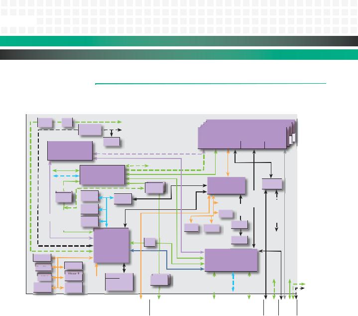


 Overview: Functional Overview
FUNCTIONAL OVERVIEW
The following block diagram provides a functional overview for the KAT4000:
Figure 1-1: General System Block Diagram
|
|
10/100 |
|
|
Xfmr |
|
|
|
|
|
|
|
|
|
|
|||||
|
|
|
|
PHY |
|
|
|
|
|
|
|
|
To Zone 3 |
|
||||||
|
|
|
|
|
|
|
|
|
|
EIA-232 |
|
|
|
|
|
|||||
|
|
|
|
|
|
|
|
|
|
|
|
|
|
|
(Optional) |
|
||||
|
|
|
|
|
|
|
|
|
|
Transceiver |
|
|
|
|
|
|
|
|
||
|
|
|
|
|
|
|
|
|
|
|
|
|
|
Serial |
|
|
|
|
||
|
|
|
|
|
|
|
PEX8524 |
|
|
Header |
|
|
|
|
||||||
|
|
|
|
|
|
|
|
|
|
|
|
|
|
|
|
|
||||
|
|
|
|
|
PCI Express Switch |
|
|
|
|
|
|
|
|
|||||||
|
|
|
|
|
|
|
(Optional) |
|
|
|
|
|
|
|
|
|
|
|||
|
|
|
|
|
|
To Zone 3 |
|
|
|
|
|
|
4 SERDES |
|
||||||
|
|
|
|
|
|
VSC7376 |
SERDES |
|
||||||||||||
|
|
|
|
|
|
|
2 SERDES |
|
|
SERDES |
|
|||||||||
|
|
|
|
|
|
|
|
|
|
|
Ethernet Core Switch |
|
||||||||
|
|
|
|
|
|
To local bus |
|
SERDES |
|
|||||||||||
|
|
|
|
|
|
|
Layer 2 (Optional) |
|
||||||||||||
|
|
|
|
|
|
|
|
|
|
|||||||||||
|
(MII) |
|
|
|
|
|
|
|
|
|
2 SGMII |
|
||||||||
|
|
|
|
|
|
|
|
|
|
|
|
|
|
|
|
|
||||
|
|
|
|
|
|
|
|
|
|
|
|
|
|
|
|
|
|
|||
|
|
|
|
|
2 SERDES |
|
|
|
|
|
|
|
|
|
|
|
||||
|
Eth |
|
|
|
|
|
|
|
|
|
|
Optional |
|
|
|
|
|
|||
|
|
1 |
|
|
|
|
|
|
|
|
|
|
|
|
|
|
||||
|
|
|
|
|
|
|
|
|
|
|
|
|
|
|
|
|
|
|
||
|
Debug |
|
Serial |
|
|
|
GbE |
|
|
|
|
|
|
|
|
|
|
|||
|
|
|
|
|
PHYs ( |
|
|
|
|
|
|
|
|
|
|
|||||
|
10/100 |
|
|
|
|
|
GMII/RGMII |
|
|
|
|
|
|
|
|
|
|
|
||
|
|
|
PCIe |
|
|
|
NAND |
|
|
|
|
|
|
|
|
|||||
|
|
|
|
|
|
|
|
|
|
|
|
|
|
|||||||
|
|
|
|
|
|
|
|
|
|
|
Flash |
|
|
|
|
|
|
|
|
|
|
|
SO-DIMM |
|
|
|
|
|
I2C |
|
|
|
|
|
|
|
|
||||
|
|
|
|
|
|
|
|
|
|
|
|
|
|
|
|
|
|
|||
|
|
|
|
|
|
|
|
Main PLD |
|
|
|
|
|
|
|
|
|
|
||
|
|
|
|
|
|
|
|
|
|
|
I2C |
|
|
|
|
|
|
|
|
|
|
|
|
|
|
|
|
SEEPROM |
To Zone 3 |
|
SROM |
|
|
|
|
Xfmr (2) |
|||||
|
|
|
|
|
|
DDR2-667 |
||||||||||||||
|
|
|
|
|
|
|
|
|
|
|
|
|
|
|||||||
|
|
CPU Init |
|
|
|
User 2 |
|
|
|
|
||||||||||
|
|
|
|
|
|
|
|
|
2GB |
|
|
|
|
|||||||
|
|
SEEPROM |
|
|
SEEPROM |
|
|
|
|
|
|
|
2 |
|
|
|||||
AMC (x4) Single-Width,
Half-/Full-/Extended-Height
|
|
|
|
|
|
|
|
|
|
|
|
|
|
|
|
|
|
|
|
|
|
|
|
|
AMC.0 Common |
|
AMC.z |
|
Extended |
|
|
|
|||||||||||||
|
|
Fat Pipes |
|
|
|
|
||||||||||||||||
PCIe or GbE |
|
|
2 |
|
|
|
|
|
|
|
|
|
|
|
|
|
|
|
|
|
|
|
|
|
|
|
C |
|
|
|
|
|
|
|
|
|
|
|
|
|
|
|
|
|
|
|
|
|
|
IPMB-L I |
|
|
|
|
|
|
|
|
|
|
|
|
|
|
|
|||
|
|
|
|
|
|
|
|
|
|
|
3 |
|
|
|
|
|
|
|
|
|||
|
|
|
|
|
|
|
|
|
|
|
|
|
|
|
|
|
|
|
||||
|
|
|
|
IPMC |
|
|
|
|
|
|
Clock |
|
|
|
|
|
||||||
|
|
|
|
|
|
|
|
|
|
|
|
|
|
|
|
|
|
|
|
|
||
|
|
|
|
To Zone 3 |
|
|
4 SERDES |
|
|
|
|
processor |
|
|
|
|
|
|
||||
|
|
|
|
|
|
|
Serial2 |
|
|
|
|
|
|
|
|
|
|
|
|
|||
|
|
|
|
-48V |
|
|
|
|
|
|
|
|
|
|
|
|
|
|||||
Private I2C |
Cnvrtr |
EIA-232 |
|
|
|
|
|
|
To |
|
|
|
|
|
|
|||||||
|
|
|
|
|
|
|
|
|
|
|
|
|
|
|||||||||
|
|
|
|
|
|
|
|
|
|
|
|
|
|
|
|
|
|
|
|
|||
|
|
Sensors |
|
|
|
Xcvr |
|
|
|
|
|
|
|
|
|
|
|
|
|
|
|
|
|
|
|
|
|
|
|
Serial |
|
|
|
|
|
|
|
|
|
|
|
|
|
|
|
|
|
|
|
|
|
Header |
|
|
|
|
4 SERDES |
|
|
|
|
|
||||||
|
|
|
|
|
|
|
|
|
|
|
|
|
(no conn. |
|
|
|
|
|
||||
|
|
Fat Pipe Switch Module |
|
|
|
for |
|
|
|
|
|
|
||||||||||
|
|
|
|
GbE) |
|
|
|
|
|
|||||||||||||
SERDES GbE |
|
Fabric Options: |
|
|
|
|
|
|
|
|
|
|
|
|
|
|
|
|||||
|
|
GbE, sRIO, |
|
|
|
|
|
|
|
|
|
|
|
|
|
|
|
|||||
|
|
10-1 GbE or 10-10 GbE |
|
|
|
|
|
|
|
To Eth |
||||||||||||
|
|
|
|
|
|
|
|
|
|
|
|
|
|
|
|
|
|
|
||||
|
|
|
|
|
|
|
|
|
|
|
|
|
|
|
|
|
|
|
|
Core |
||
|
|
4 SERDES |
|
|
|
|
|
|
4 SERDES |
|
|
|
|
|
|
|
|
Switch |
||||
|
|
|
To |
local |
bus |
|
|
|
|
|
|
|
|
|
||||||||
|
|
|
|
|
|
|
|
|
|
|
|
|
|
|||||||||
|
|
|
|
|
|
|
|
|
|
|
|
|
|
|
|
|
|
|
|
|||
|
|
|
|
|
|
|
2 |
|
|
4 |
|
|
9 |
|
2 |
|
||||||
IPMB |
Base |
High Speed |
High Speed |
Clock |
RTM I/O |
|
|
Fabric A |
Fabric B |
|
(Optional) |
P10 |
|
J23 |
|
J20 |
Zone 3 |
|
|
|
|
|
|
Zone 3
Connections
(Opt.)
10007175-02 |
KAT4000 User’s Manual |
1-5 |
|
|
|


 Overview: Physical Memory Map


PHYSICAL MEMORY MAP
Fig. 1-2 illustrates the KAT4000 memory map:
Figure 1-2: KAT4000 Memory Map
Hex Address
FFFF,FFFF
FFF0,0000
FF80,0000
FF70,0000
FC88,0000
FC80,0000
FC48,0000
FC40,0000
FC18,0000
FC14,0000
FC12,0000
FC10,0000
FC00,8000
FC00,0000
E200,0000
E000,0000
A000,0000
8000,0000
3FFF,FFFF
1FFF,FFFF
0000,0000
Boot Area (1 MB)
Reserved
CCSRBAR (MPC8548 Registers, 1 MB)
Reserved
Socketed Flash (if installed) (512 KB)
Reserved
CPLD Registers (512 KB)
Reserved
Fat Pipe Switch Registers
(if installed) (256 KB)
Reserved
Ethernet Core Switch Registers (128 KB)
Reserved
NAND Flash (32 KB)
Reserved
NOR Flash (32 MB)
PCIe Switch or sRIO Fat Pipe Module (if installed) (1 GB)
PCI Express Switch (if installed) (512 MB)
Reserved
Reserved |
SDRAM |
|
|
||
|
DDR2 |
|
SDRAM |
(1 GB) |
|
DDR2 |
||
|
||
(512 MB) |
|
Hex Address
FC40,00B0
FC40,00AC
FC40,00A8
FC40,00A4
FC40,00A0
FC40,009C
FC40,0098
FC40,0094
FC40,0090
FC40,008C
FC40,0088
FC40,0084
FC40,0080
FC40,007C
FC40,0078
FC40,0074
FC40,0070
FC40,006C
FC40,0068
FC40,0064
FC40,0060
FC40,005C
FC40,0058
FC40,0054
FC40,0050
FC40,004C
FC40,0048
FC40,0044
FC40,0040
FC40,003C
FC40,0038
FC40,0034
FC40,0030
FC40,002C
FC40,0028
FC40,0024
FC40,0020
FC40,001C
FC40,0018
FC40,0014
FC40,0010
FC40,000C
FC40,0008
FC40,0004
FC40,0000
Clock Sync. Interrupt Register 3
Clock Sync. Interrupt Register 2
Clock Sync. Interrupt Register 1
Clock Control, aTCA CLK3 B Register
Clock Control, aTCA CLK3 A Register
Clock Control, AMC4 CLK3 Register
Clock Control, AMC4 CLK2 Register
Clock Control, AMC4 CLK1 Register
Clock Control, AMC3 CLK3 Register
Clock Control, AMC3 CLK2 Register
Clock Control, AMC3 CLK1 Register
Clock Control, AMC2 CLK3 Register
Clock Control, AMC2 CLK2 Register
Clock Control, AMC2 CLK1 Register
Clock Control, AMC1 CLK3 Register
Clock Control, AMC1 CLK2 Register
Clock Control, AMC1 CLK1 Register
Reserved
Clock Sync. Secondary Source 3
Clock Sync. Secondary Source 2
Clock Sync. Secondary Source 1
Reserved
Clock Sync. Primary Source 3
Clock Sync. Primary Source 2
Clock Sync. Primary Source 1
Reserved
Clock Sync. Control Register 3
Clock Sync. Control Register 2
Clock Sync. Control Register 1
RTM GPIO Control Register
RTM GPIO State Register
MISC Control Register
Boot Device Redirection Register
Scratch Register 1
Reset Command Register 2
Reset Command Register 1
Reset Event Register
LED Control Register
Jumper Settings Register
Reserved
Hardware Config. Register 0
PLL Configuration Register
PLD Version Register
Hardware Version Register
Product ID Register
1-6 |
KAT4000 User’s Manual |
10007175-02 |
|
|
|


 Overview: Physical Memory Map


Table 1-1 summarizes the physical addresses for the KAT4000 and provides references to more detailed information:
Table 1-1: KAT4000 Address Summary
Physical |
Access |
|
|
Address (hex): |
Mode: |
Description: |
See Page: |
FFF0,0000 |
R/W |
Boot Area (1 MB) |
– |
|
|
|
|
FF80,0000 |
– |
Reserved |
– |
FF70,0000 |
W |
CCSRBAR (MPC8548 Registers, 1 MB) |
– |
FC88,0000 |
– |
Reserved1 |
– |
FC80,0000 |
R/W |
Socketed Flash (if installed) (512 KB) |
6-1 |
|
|
|
|
FC48,0000 |
– |
Reserved |
– |
FC40,00B0 |
R/W |
Clock Synchronizer Interrupt Register 3 (CSI3) |
7-18 |
|
|
|
|
FC40,00AC |
R/W |
Clock Synchronizer Interrupt Register 2 (CSI2) |
7-18 |
|
|
|
|
FC40,00A8 |
R/W |
Clock Synchronizer Interrupt Register 1 (CSI1) |
7-18 |
|
|
|
|
FC40,00A4 |
R/W |
Clock Control, aTCA CLK3 B Register (CCR14) |
7-17 |
|
|
|
|
FC40,00A0 |
R/W |
Clock Control, aTCA CLK3 A Register (CCR13) |
7-17 |
|
|
|
|
FC40,009C |
R/W |
Clock Control, AMC4 CLK3 Register (CCR12) |
7-17 |
|
|
|
|
FC40,0098 |
R/W |
Clock Control, AMC4 CLK2 Register (CCR11) |
7-17 |
|
|
|
|
FC40,0094 |
R/W |
Clock Control, AMC4 CLK1 Register (CCR10) |
7-17 |
|
|
|
|
FC40,0090 |
R/W |
Clock Control, AMC3 CLK3 Register (CCR9) |
7-17 |
|
|
|
|
FC40,008C |
R/W |
Clock Control, AMC3 CLK2 Register (CCR8) |
7-17 |
|
|
|
|
FC40,0088 |
R/W |
Clock Control, AMC3 CLK1 Register (CCR7) |
7-17 |
|
|
|
|
FC40,0084 |
R/W |
Clock Control, AMC2 CLK3 Register (CCR6) |
7-17 |
|
|
|
|
FC40,0080 |
R/W |
Clock Control, AMC2 CLK2 Register (CCR5) |
7-17 |
|
|
|
|
FC40,007C |
R/W |
Clock Control, AMC2 CLK1 Register (CCR4) |
7-17 |
|
|
|
|
FC40,0078 |
R/W |
Clock Control, AMC1 CLK3 Register (CCR3) |
7-17 |
|
|
|
|
FC40,0074 |
R/W |
Clock Control, AMC1 CLK2 Register (CCR2) |
7-17 |
|
|
|
|
FC40,0070 |
R/W |
Clock Control, AMC1 CLK1 Register (CCR1) |
7-17 |
|
|
|
|
FC40,006C |
– |
Reserved |
– |
FC40,0068 |
R/W |
Clock Synchronizer Secondary Source Register 3 (CSS3) |
7-15 |
|
|
|
|
FC40,0064 |
R/W |
Clock Synchronizer Secondary Source Register 2 (CSS2) |
7-15 |
|
|
|
|
FC40,0060 |
R/W |
Clock Synchronizer Secondary Source Register 1 (CSS1) |
7-15 |
|
|
|
|
FC40,005C |
– |
Reserved |
– |
FC40,0058 |
R/W |
Clock Synchronizer Primary Source Register 3 (CPS3) |
7-14 |
|
|
|
|
FC40,0054 |
R/W |
Clock Synchronizer Primary Source Register 2 (CPS2) |
7-14 |
|
|
|
|
FC40,0050 |
R/W |
Clock Synchronizer Primary Source Register 1 (CPS1) |
7-14 |
|
|
|
|
FC40,004C |
– |
Reserved |
– |
FC40,0048 |
R/W |
Clock Synchronizer Control Register 3 (CSC3) |
7-13 |
|
|
|
|
FC40,0044 |
R/W |
Clock Synchronizer Control Register 2 (CSC2) |
7-13 |
|
|
|
|
FC40,0040 |
R/W |
Clock Synchronizer Control Register 1 (CSC1) |
7-13 |
|
|
|
|
10007175-02 |
KAT4000 User’s Manual |
1-7 |
|
|
|


 Overview: Physical Memory Map


|
|
|
|
|
|
|
|
|
|
|
|
|
|
|
|
|
|
|
|
|
|
|
|
|
|
|
|
|
|
|
|
|
|
|
|
|
|
|
|
|
|
|
|
|
|
|
|
|
|
|
|
|
|
|
|
|
|
|
|
|
|
|
|
|
|
|
|
|
|
|
|
|
|
|
|
|
|
|
|
|
|
|
|
|
|
|
|
|
|
|
|
Physical |
|
Access |
|
|
|
|
|
|
|
|
|
|
|
|
|
|
|
|
|
|
|
|
|
|
|
|
|
|
|
|
|
|
|
|
|
|
See Page: |
|
|
|
|
|
|
|
|
|
|||||||||||||||||||||||||
|
|
|
|
|
|
|
|
|
|
|
|
|
|
|
|
|
|
|
|
|
|
|
|
|
|
|
|
|
|
|
|
|
|
|
|
|
|
|
|
|
|
|
|
|
|
|
|
|
|
|
|
|
|
||||||||||||||||||||||||||||
|
|
|
|
|
|
|
|
|
|
Address (hex): |
|
Mode: |
|
Description: |
|
(continued) |
|
|
|
|
|
|
|
|
|
||||||||||||||||||||||||||||||||||||||||||||||||||||||||
|
|
|
|
|
|
|
|
|
|
FC40,003C |
|
R/W |
|
RTM GPIO Control Register (RGCR) |
|
7-7 |
|
|
|
|
|
|
|
|
|
|
|
|
|
|
|||||||||||||||||||||||||||||||||||||||||||||||||||
|
|
|
|
|
|
|
|
|
|
|
|
|
|
|
|
|
|
|
|
|
|
|
|
|
|
|
|
|
|
|
|||||||||||||||||||||||||||||||||||||||||||||||||||
|
|
|
|
|
|
|
|
|
|
FC40,0038 |
|
R |
|
RTM GPIO State Register (RGSR) |
|
7-6 |
|
|
|
|
|
|
|
|
|
|
|
|
|
|
|||||||||||||||||||||||||||||||||||||||||||||||||||
|
|
|
|
|
|
|
|
|
|
|
|
|
|
|
|
|
|
|
|
|
|
|
|
|
|
|
|
|
|
|
|||||||||||||||||||||||||||||||||||||||||||||||||||
|
|
|
|
|
|
|
|
|
|
FC40,0034 |
|
R/W |
|
MISC Control (PCIe, SIO, I2C, Test Clock) Register (MISC) |
|
7-7 |
|
|
|
|
|
|
|
|
|
|
|
|
|
|
|||||||||||||||||||||||||||||||||||||||||||||||||||
|
|
|
|
|
|
|
|
|
|
FC40,0030 |
|
R |
|
Boot Device Redirection Register (BDRR) |
|
7-12 |
|
|
|
|
|
|
|
|
|
|
|
|
|
||||||||||||||||||||||||||||||||||||||||||||||||||||
|
|
|
|
|
|
|
|
|
|
|
|
|
|
|
|
|
|
|
|
|
|
|
|
|
|
|
|
|
|
|
|||||||||||||||||||||||||||||||||||||||||||||||||||
|
|
|
|
|
|
|
|
|
|
FC40,002C |
|
R/W |
|
Scratch Register 1 (SCR1) |
|
7-8 |
|
|
|
|
|
|
|
|
|
|
|
|
|
|
|||||||||||||||||||||||||||||||||||||||||||||||||||
|
|
|
|
|
|
|
|
|
|
|
|
|
|
|
|
|
|
|
|
|
|
|
|
|
|
|
|
|
|
||||||||||||||||||||||||||||||||||||||||||||||||||||
|
|
|
|
|
|
|
|
|
|
FC40,0028 |
|
W |
|
Reset Command Register 2 (RCR2) |
|
7-10 |
|
|
|
|
|
|
|
|
|
|
|
|
|
||||||||||||||||||||||||||||||||||||||||||||||||||||
|
|
|
|
|
|
|
|
|
|
|
|
|
|
|
|
|
|
|
|
|
|
|
|
|
|
|
|
|
|
|
|||||||||||||||||||||||||||||||||||||||||||||||||||
|
|
|
|
|
|
|
|
|
|
FC40,0024 |
|
W |
|
Reset Command Register 1 (RCR1) |
|
7-9 |
|
|
|
|
|
|
|
|
|
|
|
|
|
|
|||||||||||||||||||||||||||||||||||||||||||||||||||
|
|
|
|
|
|
|
|
|
|
|
|
|
|
|
|
|
|
|
|
|
|
|
|
|
|
|
|
|
|
|
|||||||||||||||||||||||||||||||||||||||||||||||||||
|
|
|
|
|
|
|
|
|
|
FC40,0020 |
|
R |
|
Reset Event Register (RER) |
|
7-9 |
|
|
|
|
|
|
|
|
|
|
|
|
|
|
|||||||||||||||||||||||||||||||||||||||||||||||||||
|
|
|
|
|
|
|
|
|
|
|
|
|
|
|
|
|
|
|
|
|
|
|
|
|
|
|
|
|
|
|
|||||||||||||||||||||||||||||||||||||||||||||||||||
|
|
|
|
|
|
|
|
|
|
FC40,001C |
|
R/W |
|
LED Control Register (LEDR) |
|
7-5 |
|
|
|
|
|
|
|
|
|
|
|
|
|
|
|||||||||||||||||||||||||||||||||||||||||||||||||||
|
|
|
|
|
|
|
|
|
|
|
|
|
|
|
|
|
|
|
|
|
|
|
|
|
|
|
|
|
|
|
|||||||||||||||||||||||||||||||||||||||||||||||||||
|
|
|
|
|
|
|
|
|
|
FC40,0018 |
|
R |
|
Jumper Settings Register (JSR) |
|
7-6 |
|
|
|
|
|
|
|
|
|
|
|
|
|
|
|||||||||||||||||||||||||||||||||||||||||||||||||||
|
|
|
|
|
|
|
|
|
|
|
|
|
|
|
|
|
|
|
|
|
|
|
|
|
|
||||||||||||||||||||||||||||||||||||||||||||||||||||||||
|
|
|
|
|
|
|
|
|
|
FC00,0014 |
|
– |
|
Reserved |
|
– |
|
|
|
|
|
|
|
|
|
||||||||||||||||||||||||||||||||||||||||||||||||||||||||
|
|
|
|
|
|
|
|
|
|
FC40,0010 |
|
R |
|
Hardware Configuration Register 0 (HCR0) |
|
7-4 |
|
|
|
|
|
|
|
|
|
|
|
|
|
|
|||||||||||||||||||||||||||||||||||||||||||||||||||
|
|
|
|
|
|
|
|
|
|
|
|
|
|
|
|
|
|
|
|
|
|
|
|
|
|
|
|
|
|
|
|||||||||||||||||||||||||||||||||||||||||||||||||||
|
|
|
|
|
|
|
|
|
|
FC40,000C |
|
R/W |
|
PLL Configuration Register (PLLC) |
|
7-4 |
|
|
|
|
|
|
|
|
|
|
|
|
|
|
|||||||||||||||||||||||||||||||||||||||||||||||||||
|
|
|
|
|
|
|
|
|
|
|
|
|
|
|
|
|
|
|
|
|
|
|
|
|
|
|
|
|
|
|
|||||||||||||||||||||||||||||||||||||||||||||||||||
|
|
|
|
|
|
|
|
|
|
FC40,0008 |
|
R |
|
PLD Version Register (PVR) |
|
7-3 |
|
|
|
|
|
|
|
|
|
|
|
|
|
|
|||||||||||||||||||||||||||||||||||||||||||||||||||
|
|
|
|
|
|
|
|
|
|
|
|
|
|
|
|
|
|
|
|
|
|
|
|
|
|
|
|
|
|
|
|||||||||||||||||||||||||||||||||||||||||||||||||||
|
|
|
|
|
|
|
|
|
|
FC40,0004 |
|
R |
|
Hardware Version Register (HVR) |
|
7-3 |
|
|
|
|
|
|
|
|
|
|
|
|
|
|
|||||||||||||||||||||||||||||||||||||||||||||||||||
|
|
|
|
|
|
|
|
|
|
|
|
|
|
|
|
|
|
|
|
|
|
|
|
|
|
|
|
|
|
|
|||||||||||||||||||||||||||||||||||||||||||||||||||
|
|
|
|
|
|
|
|
|
|
FC40,0000 |
|
R |
|
Product ID Register (PIDR) |
|
7-2 |
|
|
|
|
|
|
|
|
|
|
|
|
|
|
|||||||||||||||||||||||||||||||||||||||||||||||||||
|
|
|
|
|
|
|
|
|
|
|
|
|
|
|
|
|
|
|
|
|
|
|
|
|
|
||||||||||||||||||||||||||||||||||||||||||||||||||||||||
|
|
|
|
|
|
|
|
|
|
FC18,0000 |
|
– |
|
Reserved |
|
– |
|
|
|
|
|
|
|
|
|
||||||||||||||||||||||||||||||||||||||||||||||||||||||||
|
|
|
|
|
|
|
|
|
|
FC14,0000 |
|
R/W |
|
Fat Pipe Ethernet Switch Registers (if installed) (256 KB) |
|
5-2 |
|
|
|
|
|
|
|
|
|
|
|
|
|
|
|||||||||||||||||||||||||||||||||||||||||||||||||||
|
|
|
|
|
|
|
|
|
|
|
|
|
|
|
|
|
|
|
|
|
|
|
|
|
|
||||||||||||||||||||||||||||||||||||||||||||||||||||||||
|
|
|
|
|
|
|
|
|
|
FC12,0000 |
|
– |
|
Reserved |
|
– |
|
|
|
|
|
|
|
|
|
||||||||||||||||||||||||||||||||||||||||||||||||||||||||
|
|
|
|
|
|
|
|
|
|
FC10,0000 |
|
R/W |
|
Ethernet Core Switch Registers (128 KB) |
|
4-2 |
|
|
|
|
|
|
|
|
|
|
|
|
|
|
|||||||||||||||||||||||||||||||||||||||||||||||||||
|
|
|
|
|
|
|
|
|
|
|
|
|
|
|
|
|
|
|
|
|
|
|
|
|
|
||||||||||||||||||||||||||||||||||||||||||||||||||||||||
|
|
|
|
|
|
|
|
|
|
FC00,8000 |
|
– |
|
Reserved |
|
– |
|
|
|
|
|
|
|
|
|
||||||||||||||||||||||||||||||||||||||||||||||||||||||||
|
|
|
|
|
|
|
|
|
|
FC00,0000 |
|
R/W |
|
NAND Flash (32 KB) |
|
6-2 |
|
|
|
|
|
|
|
|
|
|
|
|
|
|
|||||||||||||||||||||||||||||||||||||||||||||||||||
|
|
|
|
|
|
|
|
|
|
E200,0000 |
|
– |
|
Reserved1 |
|
– |
|
|
|
|
|
|
|
|
|
||||||||||||||||||||||||||||||||||||||||||||||||||||||||
|
|
|
|
|
|
|
|
|
|
E000,0000 |
|
R/W |
|
NOR Flash (32 MB) |
|
6-1 |
|
|
|
|
|
|
|
|
|
|
|
|
|
|
|||||||||||||||||||||||||||||||||||||||||||||||||||
|
|
|
|
|
|
|
|
|
|
|
|
|
|
|
|
|
|
|
|
|
|
|
|
|
|
||||||||||||||||||||||||||||||||||||||||||||||||||||||||
|
|
|
|
|
|
|
|
|
|
A000,0000 |
|
R/W |
|
PCI Express Switch or sRIO Fat Pipe Switch Module (if installed) |
|
4-7 or 5-22 |
|
|
|
|
|
|
|
|
|
||||||||||||||||||||||||||||||||||||||||||||||||||||||||
|
|
|
|
|
|
|
|
|
|
|
|
|
|
|
|
|
|
|
|
|
|
|
|
|
|
|
|
|
|
|
|
(1 GB)2 |
|
|
|
|
|
|
|
|
|
|
|
|
|
|
|
|
|
|
|||||||||||||||||||||||||||||||
|
|
|
|
|
|
|
|
|
|
8000,0000 |
|
|
|
|
|
|
R/W |
|
PCI Express Switch (if installed) (512 MB)2 |
|
4-7 |
|
|
|
|
|
|
|
|
|
|
|
|
|
|
||||||||||||||||||||||||||||||||||||||||||||||
|
|
|
|
|
|
|
|
|
|
4000,0000 |
|
|
|
|
|
|
– |
|
Reserved1 |
|
– |
|
|
|
|
|
|
|
|
|
|||||||||||||||||||||||||||||||||||||||||||||||||||
|
|
|
|
|
|
|
|
|
|
0000,0000 |
|
|
|
|
|
|
R/W |
|
SDRAM DDR2 (512 MB/1 GB) |
|
6-2 |
|
|
|
|
|
|
|
|
|
|
|
|
|
|
||||||||||||||||||||||||||||||||||||||||||||||
|
|
|
|
|
|
|
|
|
|
|
|
|
|
|
|
|
|
|
|
|
|
|
|
|
|
|
|
|
|
|
|
|
|
|
|
|
|
|
|
|
|
|
|
|
|
|
|
|
|
|
|
|
|
|
|
|
|
|
|
|
|
|
|
|
|
|
|
|
|
|
|
|
|
|
|
|
|
|
|
|
|
1.Depends on Flash/memory size.
2.Both the PCI Express Switch and sRIO Fat Pipe Switch Module are optional. If both devices are discovered onboard, then the PCIe switch will be allocated 512 MB and the sRIO fat pipe switch module will be allocated 1 GB of addressable space. If neither device is found onboard, the entire 1.5 GB area is reserved.
1-8 |
KAT4000 User’s Manual |
10007175-02 |
|
|
|


 Overview: AMC Mapping


AMC MAPPING
The figure below shows how the KAT4000 maps to the ports defined by the AMC.0 specification:
Figure 1-3: AMC Port Mapping Regions
|
|
|
|
|
|
Port # |
|
|
Port Mapping |
||||||||||||
|
|
|
|
|
|
|
|
|
|
|
|
|
|
|
|
|
|
|
|||
|
|
|
|
|
|
|
CLK1 |
|
|
|
Clocks |
|
|
SYNCLK |
|
||||||
|
|
|
|
|
|
|
CLK2 |
|
|
|
|
|
SYNCLK |
|
|||||||
|
|
|
|
|
Basic |
|
CLK3 |
|
|
|
|
|
|
|
|
REFCLK/SYNCLK |
|
|
|
||
|
|
|
|
|
|
0 |
|
|
|
|
|
|
|
|
GbE |
|
|
||||
|
|
|
|
|
Connector |
|
1 |
|
Common Options |
PCIe or GbE |
|
||||||||||
|
|
|
|
|
|
5 |
|
|
|
Region |
|
|
below for |
|
|||||||
|
|
|
|
|
|
|
2 |
|
|
|
|
|
See below for |
|
|||||||
|
|
|
|
|
|
|
3 |
|
|
|
|
|
|
|
|
port routing |
|
||||
|
|
|
|
|
|
|
4 |
|
|
|
|
|
|
|
|
See |
|
|
|
|
|
|
|
|
|
|
|
|
|
|
|
|
|
|
|
|
|
|
|
||||
|
|
|
|
|
|
|
6 |
|
Fat Pipes Region |
|
|
configuration |
|
||||||||
|
|
|
|
|
|
|
7 |
|
|
|
options |
|
|||||||||
|
|
|
|
|
|
|
|
|
|
|
|
|
|
|
|
|
|
|
|
||
|
|
|
|
|
|
|
8 |
|
|
|
|
|
|
|
|
|
|
|
|
|
|
|
|
|
|
|
|
|
9 |
|
|
|
|
|
|
|
|
See below |
|
||||
|
|
|
|
|
Extended |
|
10 |
|
|
|
|
|
|
|
|
for port |
|
||||
|
|
|
|
|
|
|
|
|
|
|
|
|
|
routing |
|
|
|
|
|||
|
|
|
|
|
|
|
11 |
|
|
|
|
|
|
|
|
|
|
|
|
|
|
|
|
|
|
|
|
|
12 |
|
|
|
|
|
|
|
|
|
|
|
|
|
|
|
|
|
|
|
|
|
13 |
|
|
|
|
|
|
|
|
|
|
|
|
|
|
|
|
|
|
|
Connector |
|
14 |
|
|
|
|
|
|
|
|
|
|
|
|
|
|
|
|
|
|
|
|
15 |
|
Extended Options |
|
|
|
|
|
|
|||||||
|
|
|
|
|
|
|
16 |
|
|
Zone 3 |
|
|
|
|
|||||||
|
|
|
|
|
|
|
|
|
|
Region |
|
|
|
||||||||
|
|
|
|
|
|
|
|
|
|
|
|
|
|
|
|
|
|||||
|
|
|
|
|
|
|
17 |
|
|
|
|
|
|
|
|
|
|
|
|
|
|
|
|
|
|
|
|
|
18 |
|
|
|
|
|
|
|
|
|
|
|
|
|
|
|
|
|
|
|
|
|
19 |
|
|
|
|
|
|
|
|
|
|
|
|
|
|
|
|
|
|
|
|
|
20 |
|
|
|
|
|
|
|
|
|
|
|
|
|
|
|
|
|
|
|
|
|
|
|
|
AMC.0 Definition |
|
|
KAT4000 |
||||||||
|
|
|
|
|
|
|
|
|
|
|
|
|
|
|
Implementation |
||||||
|
AMC to AMC Implementation of Ports 2 and 3 |
|
|
|
GbE Fat Pipe |
||||||||||||||||
|
|
|
|
|
|
|
|
|
|
|
|
|
|
|
|
Switch Module |
|||||
|
|
|
|
|
|
|
|
|
|
|
|
|
|
|
Implementation |
||||||
|
B4 |
|
|
|
B3 |
|
B2 |
|
|
B1 |
|
|
|
|
|
|
|
|
|
||
2 |
3 |
|
2 |
3 |
|
2 |
|
3 |
|
2 |
3 |
|
|
|
|
|
|
|
|
||
|
|
|
|
|
|
|
|
|
|
|
|
|
|
|
|
sRIO Fat Pipe |
|||||
|
|
|
|
|
|
|
|
|
|
|
|
|
|
|
|
Switch Module |
|||||
|
|
|
|
|
|
|
|
|
|
|
|
|
|
|
Implementation |
||||||
|
AMC to AMC Implementation of Ports 8–11 |
|
|
|
|
|
|
|
|
|
|||||||||||
|
|
|
|
|
|
|
|
|
|
|
|
|
|
|
|
|
10-1 GbE |
||||
|
|
|
|
|
|
|
|
|
|
|
|
|
|
|
|
|
|||||
|
B4 |
|
|
|
B2 |
|
B3 |
|
|
B1 |
|
|
|
|
Fat Pipe |
||||||
|
|
|
|
|
|
|
|
|
|
Switch Module |
|||||||||||
8 9 10 11 |
|
8 9 10 11 |
|
8 9 10 11 |
|
8 9 10 11 |
|
Implementation |
|||||||||||||
|
|
|
|
|
|
|
|
|
|
|
|||||||||||
|
|
|
|
|
|
|
|
|
|
|
|
|
|
|
|
|
|
|
|
|
|
Port #
4GbE x1
5GbE x1
GbE x1
7GbE x1
Port #
4sRIO x1
5sRIO
x4
7
Port #
4GbE x1
5GbE x1
GbE x1
7GbE x1
10-10 GbE |
Port # |
|
4 |
|
|
Fat Pipe |
5 |
10 GbE |
Switch Module |
Implementation |
x4 |
|
|
|
7 |
10007175-02 |
KAT4000 User’s Manual |
1-9 |
|
|
|


 Overview: Additional Information
Clocks: This region supports a subset of the clock architecture, as defined in the AMC.0 specification.
Common Options: This region supports essential interfaces that are common across multiple Fat Pipe implementations.
Fat Pipes: This region supports data path connections including GbE, sRIO, PCIe, and 10 GbE. It can carry large amounts of data without significantly degrading the speed of transmission.
Extended Options: This region supports Rear Transition Modules. Also, it may be used to extend the Common Options and Fat Pipes Regions, when required.
x1, x2, x4: This refers to the link width of the port (the number of lanes that can be used to interconnect between two link partners).
ADDITIONAL INFORMATION
This section lists the KAT4000 hardware regulatory certifications and briefly discusses the terminology and notation conventions used in this manual. It also lists general technical references.
Mean time between failures (MTBF) has been calculated at greater than 315,816 hours for the KAT4000 and greater than 264,795 hours for the KAT4000 with a GbE fat pipe switch module. MTBFs were calculated using Method I Case 3, Telcordia Issue 1 model at 30° C.
Product Certification
The KAT4000 hardware has been tested to comply with various safety, immunity, and emissions requirements as specified by the Federal Communications Commission (FCC), Industry Canada (IC), Underwriters Laboratories Inc.® (UL), and the European Union Directives (CE mark). The following table summarizes this compliance:
Table 1-2: Regulatory Agency Compliance
Type: |
Specification: |
Safety |
IEC60950/EN60950 – Safety of Information Technology Equipment |
|
(Western Europe) |
|
UL60950, CSA C22.2 No. 60950, Third Edition – Safety of Information |
|
Technology Equipment, including Electrical Business Equipment (BI- |
|
National) |
|
AS/NZS 60950:2000 – Safety Standard for Australia and New Zealand |
|
Global IEC – CB Scheme Report IEC 60950, all country deviations |
|
|
1-10 |
KAT4000 User’s Manual |
10007175-02 |
|
|
|


 Overview: Additional Information
|
|
|
|
|
|
|
|
|
|
|
|
|
|
|
|
|
|
|
|
|
|
|
|
|
|
|
|
|
|
|
|
|
|
|
|
|
|
|
|
|
|
|
|
|
|
|
|
|
|
|
|
|
|
|
|
|
|
|
|
|
|
|
|
|
|
|
|
|
|
|
|
|
|
|
|
|
|
|
|
|
|
|
|
|
|
|
|
|
|
|
|
|
|
|
|
|
|
|
|
|
Type: |
|
Specification: (continued) |
|
|
|
|
|
|
|
|
|
|||||||||||||||||||||||||||||||||||||||||||||||
|
|
|
|
|
|
|
|
|
|
|
|
|
|
|
|
|
|
|
|
|
|
|
|
|
|
|
|
|
|
|
|||||||||||||||||||||||||||||||||||||||||||||||||
|
|
|
|
|
|
|
|
|
|
|
|
|
|
|
|
|
|
|
|
|
Environmental |
|
NEBS™: Telcordia™ GR-63 (applies to an entire system) – |
|
|
|
|
|
|
|
|
|
|||||||||||||||||||||||||||||||||||||||||||||||
|
|
|
|
|
|
|
|
|
|
|
|
|
|
|
|
|
|
|
|
|
|
|
|
|
|
|
|
|
|
|
|
|
|
Section 4.3 Equipment Handling Criteria; |
|
|
|
|
|
|
|
|
|
||||||||||||||||||||||||||||||||||||
|
|
|
|
|
|
|
|
|
|
|
|
|
|
|
|
|
|
|
|
|
|
|
|
|
|
|
|
|
|
|
|
|
|
Section 4.4.1 Earthquake Environment and Criteria (Zone 4); |
|
|
|
|
|
|
|
|
|
||||||||||||||||||||||||||||||||||||
|
|
|
|
|
|
|
|
|
|
|
|
|
|
|
|
|
|
|
|
|
|
|
|
|
|
|
|
|
|
|
|
|
|
Section 4.4.3 Office Vibration Environment and Criteria; |
|
|
|
|
|
|
|
|
|
||||||||||||||||||||||||||||||||||||
|
|
|
|
|
|
|
|
|
|
|
|
|
|
|
|
|
|
|
|
|
|
|
|
|
|
|
|
|
|
|
|
|
|
Section 4.4.4 Transportation Vibration Criteria |
|
|
|
|
|
|
|
|
|
||||||||||||||||||||||||||||||||||||
|
|
|
|
|
|
|
|
|
|
|
|
|
|
|
|
|
|
|
|
|
|
|
|
|
|
|
|
|
|
|
|
|
|||||||||||||||||||||||||||||||||||||||||||||||
|
|
|
|
|
|
|
|
|
|
|
|
|
|
|
|
|
|
|
|
|
EMC |
|
FCC Part 15, Class B – Title 47, Code of Federal Regulations, Radio |
|
|
|
|
|
|
|
|
|
|||||||||||||||||||||||||||||||||||||||||||||||
|
|
|
|
|
|
|
|
|
|
|
|
|
|
|
|
|
|
|
|
|
|
|
|
|
|
|
|
|
|
|
|
|
Frequency Devices |
|
|
|
|
|
|
|
|
|
|||||||||||||||||||||||||||||||||||||
|
|
|
|
|
|
|
|
|
|
|
|
|
|
|
|
|
|
|
|
|
|
|
|
|
|
|
|
|
|
|
|
|
ICES 003, Class A – Industry Canada Interference-causing Equipment |
|
|
|
|
|
|
|
|
|
|||||||||||||||||||||||||||||||||||||
|
|
|
|
|
|
|
|
|
|
|
|
|
|
|
|
|
|
|
|
|
|
|
|
|
|
|
|
|
|
|
|
|
Standard for Digital Apparatus |
|
|
|
|
|
|
|
|
|
|||||||||||||||||||||||||||||||||||||
|
|
|
|
|
|
|
|
|
|
|
|
|
|
|
|
|
|
|
|
|
|
|
|
|
|
|
|
|
|
|
|
|
NEBS: Telcordia GR-1089 level 3 – Emissions and Immunity (circuit pack |
|
|
|
|
|
|
|
|
|
|||||||||||||||||||||||||||||||||||||
|
|
|
|
|
|
|
|
|
|
|
|
|
|
|
|
|
|
|
|
|
|
|
|
|
|
|
|
|
|
|
|
|
level testing only) |
|
|
|
|
|
|
|
|
|
|||||||||||||||||||||||||||||||||||||
|
|
|
|
|
|
|
|
|
|
|
|
|
|
|
|
|
|
|
|
|
|
|
|
|
|
|
|
|
|
|
|
|
EN300386 – Electromagnetic Compatibility and Radio Spectrum Matters |
|
|
|
|
|
|
|
|
|
|||||||||||||||||||||||||||||||||||||
|
|
|
|
|
|
|
|
|
|
|
|
|
|
|
|
|
|
|
|
|
|
|
|
|
|
|
|
|
|
|
|
|
(ERM), Telecommunication Network Equipment, Electromagnetic |
|
|
|
|
|
|
|
|
|
|||||||||||||||||||||||||||||||||||||
|
|
|
|
|
|
|
|
|
|
|
|
|
|
|
|
|
|
|
|
|
|
|
|
|
|
|
|
|
|
|
|
|
Compatibility (EMC) Requirements |
|
|
|
|
|
|
|
|
|
|||||||||||||||||||||||||||||||||||||
|
|
|
|
|
|
|
|
|
|
|
|
|
|
|
|
|
|
|
|
|
|
|
|
|
|
|
|
|
|
|
|
|
AS/NZS 3548 003 – Standard for radiated and conducted emissions for |
|
|
|
|
|
|
|
|
|
|||||||||||||||||||||||||||||||||||||
|
|
|
|
|
|
|
|
|
|
|
|
|
|
|
|
|
|
|
|
|
|
|
|
|
|
|
|
|
|
|
|
|
Australia and New Zealand, Class A |
|
|
|
|
|
|
|
|
|
|||||||||||||||||||||||||||||||||||||
|
|
|
|
|
|
|
|
|
|
|
|
|
|
|
|
|
|
|
|
|
|
|
|
|
|
|
|
|
|
|
|
|
|
|
|
|
|
|
|
|
|
|
|
|
|
|
|
|
|
|
|
|
|
|
|
|
|
|
|
|
|
|
|
|
|
|
|
|
|
|
|
|
|
|
|
|
|
|
|
Emerson maintains test reports that provide specific information regarding the methods and equipment used in compliance testing. Unshielded external I/O cables, loose screws, or a poorly grounded chassis may adversely affect the KAT4000’s ability to comply with any of the stated specifications.
UL Certification
The UL web site at ul.com has a list of Emerson’s UL certifications.
1To find the list, go to the web site and search in the online certifications directory using Emerson’s UL file number, E190079. There is a list for products distributed in the United States, as well as a list for products shipped to Canada.
2Products are listed by board type followed by the model name and/or number. The KAT4000 is an AdvancedTCA (ATCA) blade. The model number is KAT4000’s Printed Circuit Board (PCB) artwork number, which is 10007505-xx.
RoHS Compliance
The KAT4000, all fat pipe modules listed in Chapter 5, and the RTM described in Chapter 13 are compliant with the European Union’s RoHS (Restriction of Use of Hazardous Substances) directive created to limit harm to the environment and human health by restricting the use of harmful substances in electrical and electronic equipment. Effective July 1, 2006, RoHS restricts the use of six substances: cadmium (Cd), mercury (Hg), hexavalent chromium (Cr (VI)), polybrominated biphenyls (PBBs), polybrominated diphenyl ethers
10007175-02 |
KAT4000 User’s Manual |
1-11 |
|
|
|


 Overview: Additional Information
(PBDEs) and lead (Pb). Configurations that are RoHS compliant are built with lead-free solder. Configurations that are 5-of-6 are built with tin-lead solder per the lead-in-solder RoHS exemption.
To obtain a certificate of conformity (CoC) for the KAT4000 or other modules, send an e- mail to sales@artesyncp.com or call 1-800-356-9602. Have the part number(s) (e.g., C000####-##) for your configuration(s) available when contacting Emerson.
Terminology and Notation
Active low signals: An active low signal is indicated with an asterisk * after the signal name.
Byte, word: Throughout this manual byte refers to 8 bits, word refers to 16 bits, and long word refers to 32 bits, double long word refers to 64 bits.
PLD: This manual uses the acronym, PLD, as a generic term for programmable logic device (also known as FPGA, CPLD, EPLD, etc.).
Radix 2 and 16: Hexadecimal numbers end with a subscript 16 or begin with 0x. Binary numbers are shown with a subscript 2.
Technical References
Further information on basic operation and programming of the KAT4000 components can be found in the following documents:
Table 1-3: Technical References
Device / Interface: |
Document: 3 |
AMC/ATCA |
Advanced Mezzanine Card Base Specification |
|
(PICMG® AMC.0 Rev. 2.0: November 15, 2006) |
|
PCI Express and Advanced Switching on AdvancedMC |
|
(PICMG® AMC.1 Rev. 1.0: January 20, 2005) |
|
AdvancedTCA® Base Specification |
|
(PICMG® 3.0 Rev. 2.0: March 18, 2005) |
|
Engineering Change Notice 3.0-2.0-001 |
|
(PICMG® 3.0 Rev. 2.0: ECN 3.0-2.0-001; June 15, 2005) |
|
AdvancedTCA® Ethernet/Fibre Channel for AdvancedTCA® Systems |
|
(PICMG® 3.1 Rev. 1.0: January 22, 2003) |
|
http://www.picmg.org |
|
|
CPLD |
MAX®II Device Handbook |
|
(Altera® MII5V1-1.3, Preliminary; December 2004) |
|
http://www.altera.com |
|
|
1-12 |
KAT4000 User’s Manual |
10007175-02 |
|
|
|
Loading...