


 Loading...
 Ver. 1
SERVICE MANUAL
MODEL |
JP |
E3 |
E2 |
EK |
E2A |
E1C |
E1K |
EUT |
|
|
|
|
|
|
|
|
|
|
|
|
|
|
|
|
|
|
TU-604CI |
|
3 |
3 |
|
|
|
|
|
|
|
|
|
|
|
|
|
|
AM-FM / XM MULTIPLE TUNER
●For purposes of improvement, specifications and design are subject to change without notice.
●Please use this service manual with referring to the operating instructions without fail.
●Some illustrations using in this service manual are slightly different from the actual set.
|
●8
e
Denon Brand Company, D&M Holdings lnc.
X0369 V.01 DE/CDM 0805
SAFETY PRECAUTIONS
The following check should be performed for the continued protection of the customer and service technician.
LEAKAGE CURRENT CHECK
Before returning the unit to the customer, make sure you make either (1) a leakage current check or (2) a line to chassis resistance check. If the leakage current exceeds 0.5 milliamps, or if the resistance from chassis to either side of the power cord is less than 460 kohms, the unit is defective.
CAUTION Please heed the points listed below during servicing and inspection.
Heed the cautions!
Spots requiring particular attention when servicing, such as the cabinet, parts, chassis, etc., have cautions indicated on labels or seals. Be sure to heed these cautions and the cautions indicated in the handling instructions.
Caution concerning electric shock!
(1)An AC voltage is impressed on this set, so touching internal metal parts when the set is energized could cause electric shock. Take care to avoid electric shock, by for example using an isolating transformer and gloves when servicing while the set is energized, unplugging the power cord when replacing parts, etc.
(2)There are high voltage parts inside. Handle with extra care when the set is energized.
Caution concerning disassembly and assembly!
Though great care is taken when manufacturing parts from sheet metal, there may in some rare cases be burrs on the edges of parts which could cause injury if fingers are moved across them. Use gloves to protect your hands.
Only use designated parts!
The set's parts have specific safety properties (fire resistance, voltage resistance, etc.). For replacement parts, be sure to use parts which have the same properties. In particular, for the important safety parts that are marked z on wiring diagrams and parts lists, be sure to use the designated parts.
Be sure to mount parts and arrange the wires as they were originally!
For safety reasons, some parts use tape, tubes or other insulating materials, and some parts are mounted away from the surface of printed circuit boards. Care is also taken with the positions of the wires inside and clamps are used to keep wires away from heating and high voltage parts, so be sure to set everything back as it was originally.
Inspect for safety after servicing!
Check that all screws, parts and wires removed or disconnected for servicing have been put back in their original positions, inspect that no parts around the area that has been serviced have been negatively affected, conduct an insulation check on the external metal connectors and between the blades of the power plug, and otherwise check that safety is ensured.
(Insulation check procedure)
Unplug the power cord from the power outlet, disconnect the antenna, plugs, etc., and turn the power switch on. Using a 500V insulation resistance tester, check that the insulation resistance between the terminals of the power plug and the externally exposed metal parts (antenna terminal, headphones terminal, microphone terminal, input terminal, etc.) is 1MΩ or greater. If it is less, the set must be inspected and repaired.
CAUTION Concerning important safety parts
Many of the electric and structural parts used in the set have special safety properties. In most cases these properties are difficult to distinguish by sight, and using replacement parts with higher ratings (rated power and withstand voltage) does not necessarily guarantee that safety performance will be preserved. Parts with safety properties are indicated as shown below on the wiring diagrams and parts lists is this service manual. Be sure to replace them with parts with the designated part number.
(1)Schematic diagrams ... Indicated by the z mark.
(2)Parts lists ... Indicated by the z mark.
Using parts other than the designated parts could result in electric shock, fires or other dangerous situations.
2 TU-604CI
|
|
|
|
|
|
|
|
|
|
|
|
|
|
|
|
|
|
|
||
(1) |
||
|
||
|
||
500V |
||
|
||
|
||
|
||
|
||
|
||
MΩ |
||
|
(2) には十分ご注意ください。
図、部品表にz
が維持されるとは、限りません。安全上の特性を持った部 品は、このサービスマニュアルの配線図、部品表につぎの ように表示していますので必ず指定されている部品番号 のものを使用願います。
(1) … z
(2) … z
3 TU-604CI
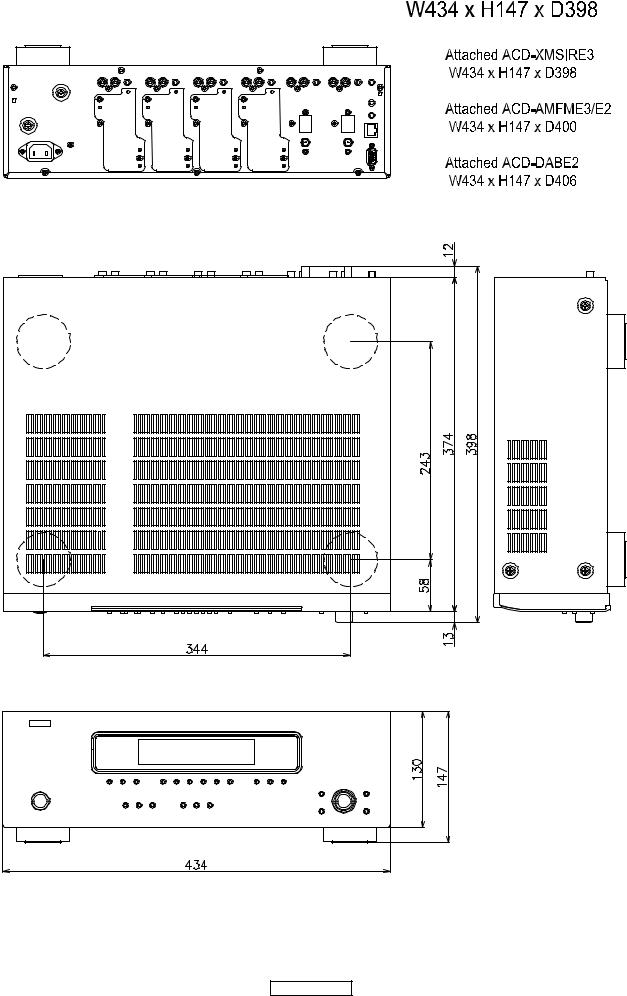
DIMENSION
4 TU-604CI
WIRE ARRANGEMENT |
|
If wire bundles are untied or moved to perform adjustment or |
|
parts replacement etc., be sure to rearrange them neatly as |
|
they were originally bundled or placed afterward. |
|
Otherwise, incorrect arrangement can be a cause of noise |
|
generation.
Wire arrangement viewed from the top |
|
|
Back Panel side |
Front Panel side
5 TU-604CI
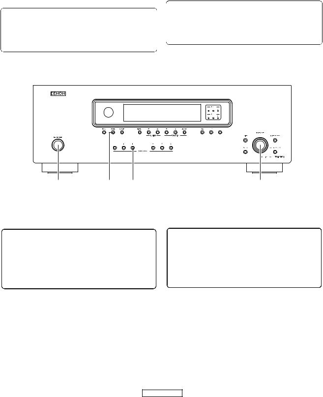
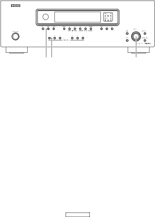
CAUTION IN SERVICING |
|
Initializing MULTI TUNER |
|
MULTI TUNER initialization should be performed when the |
Digital |
µcom and peripheral parts of µcom, and Digital P.W.B. are re- |
|
placed. |
|
1.Press the “ON/STANDBY” button, starting state it does.
2.Press the “SELECT/ENTER” button and hold it in for at least 3 seconds, while simultaneously pressing the “MODE” button and the “TUNER 3” button.
3.Check that the entire display is flashing with an interval of about 1 second, and release your fingers from the 2 buttons.
The microprocessor will be initialized.
Note: If step 3 does not work, start over from step 1.
All user settings will be lost and this factory setting will be recovered when this initialization mode. So make sure to m+emorize your setting for restoring after the initialization.
1."ON/STANDBY"
2."MODE" "TUNER 3""SELECT/ENTER" 3
3.1 2
: 3 1
ON / STANDBY |
MODE TUNER 3 |
SELECT / ENTER |
● The parts of Option board are not serviceable. |
● Option board |
Please replace the product itself. |
|
<Option board> |
<Option board> |
• ACD-AMFM |
ACD-AMFM |
• ACD-XMSIR |
ACD-XMSIR |
• ACD-HD |
ACD-HD |
• ACD-DAB |
ACD-DAB |
6 TU-604CI
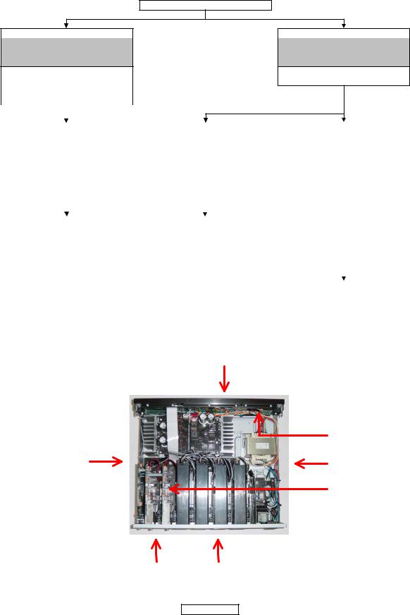
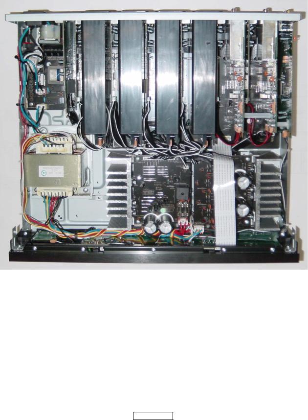
DISASSEMBLY
•Disassemble in order of the arrow of the figure of following flow.
•In the case of the re-assembling, assemble it in order of the reverse of the following flow.
•In the case of the re-assembling, observe "attention of assembling" it.
CABINET TOP
PANEL FRONT SUB ASSY
Refer to "DISASSEMBLY
1.PANEL FRONT SUB ASSY" and "EXPLODED VIEW"
POWERON UNIT
(Ref. No. of EXPLODED VIEW : 7)
FRONT P.W.B UNIT
(Ref. No. of EXPLODED VIEW : 10)
CHASSIS BACK SUB ASSY
Refer to "DISASSEMBLY
4.CHASSIS BACK SUB ASSY" and "EXPLODED VIEW"
AMFM BUILT-IN P.W.B UNIT ASSY
(Ref. No. of EXPLODED VIEW : 42)
|
|
|
|
|
|
|
|
|
|
|
|
|
|
|
|
|
|
|
|
|
|
|
|
|
|
|
HEAT SINK MAIN L SUB ASSY |
|
|
STBY UNIT ASSY |
|
IO OPTION UNIT / |
|||
Refer to "DISASSEMBLY |
|
|
Refer to "DISASSEMBLY |
|
IO BUILT-IN UNIT / |
|||
2.HEAT SINK MAIN L SUB ASSY" |
|
|
7.STBY UNIT ASSY |
|
ETHERNET P.W.B UNIT ASSY |
|||
and "EXPLODED VIEW" |
|
|
and "EXPLODED VIEW" |
|
Refer to "DISASSEMBLY |
|||
POWER2 UNIT |
|
|
STBY1 UNIT |
|
5.IO OPTION UNIT / |
|||
(Ref. No. of EXPLODED VIEW : 16) |
|
|
(Ref. No. of EXPLODED VIEW : 33) |
|
IO BUILT-IN UNIT / |
|||
POWER3 UNIT |
|
|
STBY2 UNIT |
|
ETHERNET P.W.B UNIT ASSY" |
|||
(Ref. No. of EXPLODED VIEW : 17) |
|
|
(Ref. No. of EXPLODED VIEW : 34) |
|
and "EXPLODED VIEW" |
|||
|
|
|
|
|
|
|
IO OPTION UNIT |
|
|
|
|
|
|
|
|
(Ref. No. of EXPLODED VIEW : 35) |
|
|
|
|
|
|
|
|
||
HEAT SINK MAIN R SUB ASSY |
|
|
TRANS |
|
IO BUILT-IN UNIT |
|||
Refer to "DISASSEMBLY |
|
|
Refer to "DISASSEMBLY |
|
(Ref. No. of EXPLODED VIEW : 36) |
|||
3.HEAT SINK MAIN R SUB ASSY" |
|
|
8.TRANS" |
|
ETHERNET P.W.B UNIT ASSY |
|||
and "EXPLODED VIEW" |
|
|
and "EXPLODED VIEW" |
|
(Ref. No. of EXPLODED VIEW : 37) |
|||
POWER1 UNIT |
|
|
TRANS |
|
|
|
||
(Ref. No. of EXPLODED VIEW : 15) |
|
|
(Ref. No. of EXPLODED VIEW : 28) |
|
|
|
||
XMBUS UNIT |
|
|
|
|
|
|
|
|
|
|
|
|
|
|
|
||
(Ref. No. of EXPLODED VIEW : 18) |
|
|
|
|
|
MAIN P.W.B UNIT ASSY |
||
|
|
|
|
|
|
|
Refer to "DISASSEMBLY |
|
|
|
|
|
|
|
|
6.MAIN P.W.B UNIT ASSY |
|
|
|
|
|
|
|
|
and "EXPLODED VIEW" |
|
|
|
|
|
|
|
|
MAIN P.W.B UNIT ASSY |
|
|
|
|
|
|
|
|
(Ref. No. of EXPLODED VIEW : 30) |
|
The viewpoint of each photograph |
Picture A |
(photography direction) |
|
( ) Front side |
|
Top view |
Picture F |
|
|
Picture C |
Picture D |
|
Picture G |
Picture E |
Picture B |
7 TU-604CI
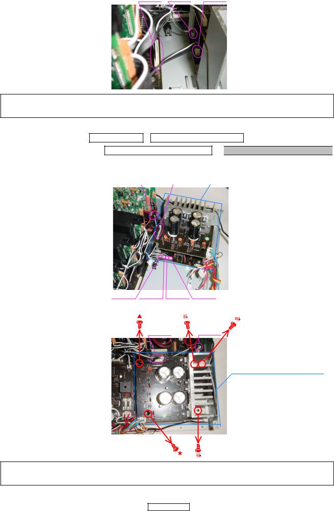
1. PANEL FRONT SUB ASSY
proceeding ( ) : CABINET TOP → PANEL FRONT SUB ASSY
(1) Remove the screws.
Bottom view
(2) Disconnect the connector wires and remove the screw.
CP1003 CP1001
Picture F
CORD HOLDER : Loose
CORD HOLDER : Loose
FFC CABLE
Picture C
CP1102
cut |
Please refer to "EXPLODED VIEW " for the disassembly method of each P.W.B included in PANEL FRONT SUB ASSY .
PANEL FRONT SUB ASSY "EXPLODED VIEW "
8 TU-604CI
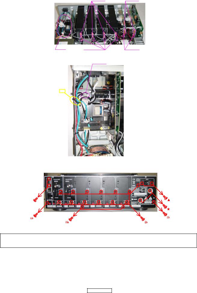
2. HEAT SINK MAIN L SUB ASSY
proceeding ( ) : CABINET TOP → PANEL FRONT SUB ASSY
→ HEAT SINK MAIN L SUB ASSY
(1)Disconnect the connector wires.
HEAT SINK MAIN R SUB ASSY
Picture A
 (A)
(A)
HEAT SINK MAIN L SUB ASSY
Detail : (A) |
CP304 |
|
CP303 |
Picture A
CP302 CN303 CN302 CP301 CP305
(2) Disconnect the connector wires and remove the screws.
(B) |
CP307 |
CP306 |
|
HEAT SINK MAIN L SUB ASSY
Top view
9 TU-604CI
(3) Disconnect the connector wires.
Detail : (B) |
CP118 |
CN311 |
CP308 |
Picture D
Please refer to "EXPLODED VIEW " for the disassembly method of each P.W.B included in HEAT SINK MAIN L SUB ASSY .
HEAT SINK MAIN L SUB ASSY "EXPLODED VIEW "
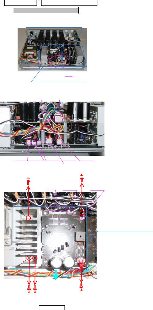
3. HEAT SINK MAIN R SUB ASSY
proceeding ( ) : CABINET TOP → PANEL FRONT SUB ASSY
→HEAT SINK MAIN L SUB ASSY → HEAT SINK MAIN R SUB ASSY
(1)Disconnect the connector wires.
CP119 |
|
CP309 |
|
HEAT SINK MAIN R SUB ASSY |
Picture D
CN304 CN305 CN307 CN308
(2) Disconnect the connector wires and remove the screws.
CP309 CP119
HEAT SINK MAIN R SUB ASSY
Top view
Please refer to "EXPLODED VIEW " for the disassembly method of each P.W.B included in HEAT SINK MAIN R SUB ASSY .
HEAT SINK MAIN R SUB ASSY "EXPLODED VIEW "
10 TU-604CI
4. CHASSIS BACK SUB ASSY
proceeding ( ) : CABINET TOP →  CHASSIS BACK SUB ASSY
Top view
CHASSIS BACK SUB ASSY
AMFM BUILT-IN P.W.B UNIT ASSY
(1) Remove the P.W.B HOLDER and disconnect the connector wire. P.W.B
P.W.B HOLDER |
AMFM BUILT-IN P.W.B UNIT ASSY |
Picture C
CP1102 ETHERNET P.W.B UNIT ASSY
11 TU-604CI
(2) Disconnect the connect wires.
CN401 CP602
Picture A
(A) |
CN402 |
CP603 |
Detail : (A) |
CP456 |
|
cut
Top view
(3) Remove the screws.
Picture B
Please refer to "EXPLODED VIEW " for the disassembly method of each P.W.B included in CHASSIS BACK SUB ASSY .
CHASSIS BACK SUB ASSY "EXPLODED VIEW "
12 TU-604CI
5. IO OPTION UNIT / IO BUILT-IN UNIT / ETHERNET P.W.B UNIT ASSY
proceeding ( ) : CABINET TOP → CHASSIS BACK SUB ASSY
→ IO OPTION UNIT / IO BUILT-IN UNIT / ETHERNET P.W.B UNIT ASSY
(1)Remove the IO OPTION UNIT , IO BUILT-IN UNIT and ETHERNET UNIT. IO OPTION UNIT IO BUILT-IN UNIT
ETHERNET UNIT
ETHERNET P.W.B UNIT ASSY |
|
IO OPTION UNIT |
CP405 |
Picture B
CP1101 |
IO BUILT-IN UNIT CP404 |
CP407 |
6. MAIN P.W.B UNIT ASSY
proceeding ( ) : CABINET TOP → CHASSIS BACK SUB ASSY
→IO OPTION UNIT / IO BUILT-IN UNIT / ETHERNET P.W.B UNIT ASSY
→ MAIN P.W.B UNIT ASSY
Please refer to "EXPLODED VIEW " for the disassembly method of MAIN P.W.B UNIT ASSY.
MAIN P.W.B UNIT ASSY "EXPLODED VIEW "
7. STBY UNIT ASSY
proceeding ( ) : CABINET TOP → CHASSIS BACK SUB ASSY
→ STBY UNIT ASSY
(1)Disconnect the connector wires and FFC Cables. FFC
STBY1 UNIT
Picture B
MAIN P.W.B UNIT ASSY |
STBY2 UNIT |
Please refer to "EXPLODED VIEW " for the disassembly method of each P.W.B included in STBY UNIT ASSY.
STBY UNIT ASSY "EXPLODED VIEW "
13 TU-604CI
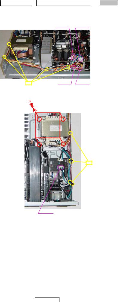
8. TRANS
proceeding ( ) : CABINET TOP → PANEL FRONT SUB ASSY →  TRANS
TRANS
(1)Remove the PANEL FRONT ASSY. PANEL FRONT ASSY
(2)Disconnect the connector wires.
CP304 CP303
Picture A
cut |
CP301 |
CP305 |
(3) Disconnect the connector wires and remove the screws.
Picture B
cut |
CP453
14 TU-604CI
CHECK WITH TEST MODE
1.Operation Spec
When the following conditions are satisfied at its starting state, error information is displayed.
Starting method (µcom version display mode):
Press the “SELECT/ENTER” button and hold it in for at least 3 seconds, while simultaneously pressing the “MODE” button and the “TUNER 1” button.
Then, “SELECT/ENTER” JOG is turned clockwise and the following information is displayed on FL Display.
2.Display Order
Destination information →Main-µcom version information → Sub-µcom version information → Ethernet information
( ):
"MODE" "TUNER 1""SELECT/ENTER" 3
"SELECT/ENTER" JOG FL Display
→ →→
MODE TUNER 1 |
SELECT / ENTER |
15 TU-604CI

---MEMO---
16 TU-604CI
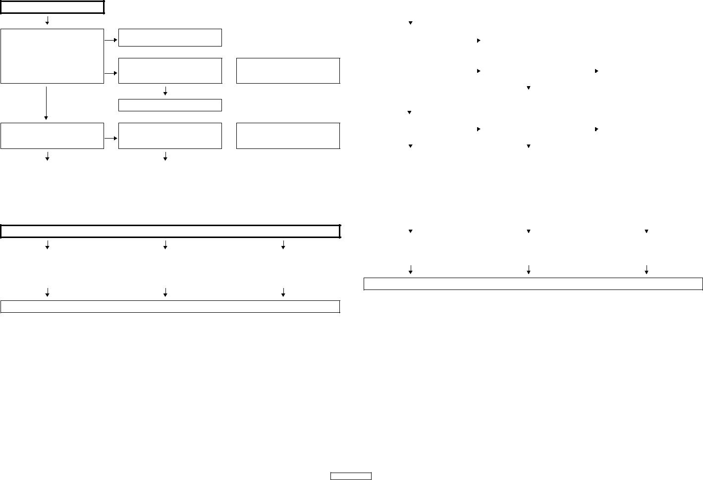
TROUBLE SHOOTING
1.POWER
1.1.Power not turn on
Power not turn on
NO
Is the fuse blown?
YES
YES
Is DC3.3V voltage supplied to the µcom? NO
YES
Refer to Fuse is blown.
Are there any incomplete connections in the connectors connecting between the various circuit boards?
YES
Connect the connectors properly.
Is a DC3.3V voltage output when the cord supplying the power to the µcom is unplugged?
YES
Check the µcom periphery circuitry and |
|
Check the circuitry and parts the |
µcom |
|
for damage and short-circuits, and |
||
replace any defective parts. |
|
||
|
replace any defective parts. |
|
|
|
|
|
|
|
|
|
|
NO Check for damage of the circuitry parts  and replace any defective parts.
NO Check the parts from µcom to the primary  circuitry and replace any defective parts.
1.2. Fuse is blown
Fuse is blown
Check for leaks or short circuits in the pri- |
|
Check for short circuits in the rectifier |
|
Check for short circuits in the power stabi- |
|
diodes and circuitry of the secondary side |
|
lizer unit's regulator output terminal and |
|
mary side parts, and replace any defec- |
|
|
||
|
rectifying circuits, and replace any defec- |
|
the ground, and replace any defective |
|
tive parts. |
|
|
||
|
tive parts. |
|
parts. |
|
|
|
|
||
|
|
|
|
|
After repairing, also replace the fuse.
|
|
|
|
|
|
|
|
|
|
|
|
|
|
|
|
NO |
|
|
|
|
|
|
|
|
|
|
|
|
|
|
|
|
|
|
|
|
||
|
|
|
|
|
|
|
|
|
|
|
||
|
|
|
|
|
|
|
|
|
|
|
||
|
|
|
|
|
|
|
|
|
|
|||
|
|
|
|
|
|
|
|
|
|
|
||
|
|
|
|
|
|
|
|
|
||||
|
|
|
|
|
|
|
|
|
|
|
||
|
|
|
|
|
|
|
|
|
|
|
||
|
|
|
YES |
|
|
|
NO |
|
|
|
||
|
|
|
|
|
|
|
||||||
|
|
|
|
|
|
|
|
|
|
|
||
|
|
|
|
|
|
|
|
|
||||
|
|
|
|
|
|
|
|
|
|
|
|
|
|
|
YES |
|
YES |
|
|
|
|
|
|
||
|
|
|
|
|
|
|
|
|
||||
|
|
|
|
|
|
|
|
|
||||
|
|
|
|
|
|
|
|
|
|
|||
|
|
|
|
|
|
|
|
|
||||
|
|
|
NO |
|
|
|
NO |
|
|
|||
|
|
|
|
|
|
|
|
|||||
|
|
|
|
|
|
|
|
|||||
|
DC3.3V |
|
|
1 |
||||||||
|
|
|
|
DC3.3V |
|
|
|
|
|
|||
|
|
|
|
|
|
|
||||||
|
|
|
|
|
|
|
|
|
|
|
|
|
|
|
YES |
|
YES |
|
|
|
|
|
|
||
|
|
|
|
|
|
|
|
|
||||
|
|
|
|
|
|
|
|
|
||||
|
|
|
|
|
|
|
|
|
|
|
|
|
|
|
|
|
|
|
|
|
|
|
|
||
|
|
|
|
|
|
|
|
|
|
|||
|
|
|
|
|
|
|
|
|
|
|||
|
|
|
|
|
|
|
|
|
|
|||
|
|
|
|
|
|
|
|
|
|
|
||
|
|
|
|
|
|
|
|
|
|
|
|
|
1.2. |
|
|
|
|
|
|
|
|
||||
|
|
|
|
|
|
|
|
|
|
|
|
|
|
|
|
|
|
|
|
|
|
|
|
|
|
|
|
|
|
|
|
|
|
|
|
|
|
|
|
|
|
|
|
|
|
|
|
|
|
|
|
|
|
|
|
|
|
|
|
|
|
|
|
|
|
|
|
|
|
|
|
|
|
|
|
|
|
|
1 |
|
|
2 |
|
|
|
|
|
|||
|
|
|
|
|
|
|
|
GND |
||||
|
|
|
|
|
|
|
|
|||||
|
|
|
|
|
|
|
|
|
||||
|
|
|
|
|
|
|
|
|
||||
|
|
|
|
|
|
|
|
|
|
|
|
|
FUSE
17 TU-604CI

BLOCK DIAGRAM
18 |
TU-604CI |
SEMICONDUCTORS
Only major semiconductors are shown, general semiconductors etc. are omitted to list.
1. IC’s
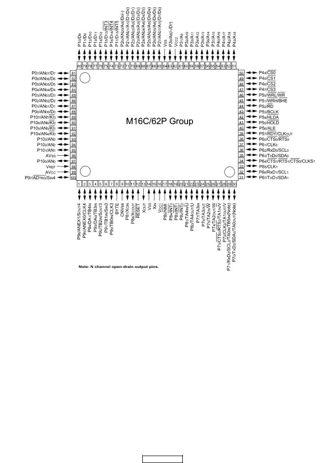
M30626FJPFP (IC103)
M30626FJPFP Terminal Function
Pin |
Pin |
Pin Name |
I/O |
STBY |
STOP |
Active |
Function |
|
Function |
||||||||
|
|
|
|
|
|
|
||
|
|
|
|
|
|
|
|
|
1 |
P96/SOUT4 |
VFD_DT |
O |
O/L |
O/L |
SERIAL |
FLD driver control terminal (16-ST-87GINK) DATA |
|
2 |
P95/CLK4 |
VFD_CLK |
O |
O/L |
O/L |
SERIAL |
FLD driver control terminal (16-ST-87GINK) CLOCK |
|
3 |
P94/TB4 |
FLD_RST |
O |
O/L |
O/L |
L:RESET |
FLD driver reset control terminal (16-ST-87GINK) |
|
|
|
|
|
|
|
|
RESET |
|
4 |
P93/TB3 |
VFD_CS |
O |
O/L |
O/L |
H:DATA transfer |
FLD driver control terminal (16-ST-87GINK) CIP |
|
|
|
|
|
|
|
prohibition |
SELECT |
|
5 |
P92/SOUT3 |
ETHER_SPI_TX(MOEI) |
O |
O/L |
O/L |
SERIAL |
ETHER SPI communication control terminal TX |
|
6 |
P91/SIN3 |
ETHER_SPI_RX(MIEO) |
I |
O/L |
O/L |
SERIAL |
ETHER SPI communication control terminal RX |
|
7 |
P90/CLK3 |
ETHER_SPI_CLK |
O |
O/L |
O/L |
SERIAL |
ETHER SPI communication control terminal CLOCK |
|
8 |
BYTE |
BYTE |
GND |
- |
- |
|
Single chip mode setting |
|
9 |
CNVCS |
CNVSS |
- |
- |
- |
|
UP GRADE PIN |
|
10 |
P87 |
MAIN_PWR_STNDBY |
O |
O/L |
O/L |
H:ACTIVE |
POWER RELAY CONTROL |
|
11 |
P86 |
NC |
O |
O/L |
O/L |
- |
PULL-DOWN |
|
12 |
RESET |
HARD RST |
I |
I |
I |
Lv |
u-COM RESET SIGNAL INPUT |
19 TU-604CI

Pin |
Pin |
Pin Name |
I/O |
STBY |
STOP |
Active |
Function |
|
Function |
||||||||
|
|
|
|
|
|
|
||
|
|
|
|
|
|
|
|
|
13 |
XOUT |
XOUT |
O |
- |
- |
|
OSILATOR CONNECTION |
|
14 |
VSS |
Vss |
GND |
- |
- |
|
GND |
|
15 |
XIN |
XIN |
I |
I |
I |
|
OSILATOR CONNECTION |
|
16 |
VCC |
Vcc1 |
3.3V |
- |
- |
|
POWER 3.3V |
|
17 |
P85/NMI |
NMI |
I |
- |
- |
|
UP GRADE PIN |
|
18 |
P84/INT2 |
PWR_DOWN |
I |
I |
I |
Fall Edge&L |
Power failure detection |
|
19 |
P83/INT1 |
REMOCON |
I |
I |
I |
Rise Edge&H |
Remote control receiver terminal |
|
20 |
P82/INT0 |
ETHER_REQ |
I |
I |
I |
Fall Edge&L |
EATHERNET REQUEST |
|
21 |
P81 |
NC |
O |
O/L |
O/L |
- |
PULL-DOWN |
|
22 |
P80 |
NC |
O |
O/L |
O/L |
- |
PULL-DOWN |
|
23 |
P77 |
NC |
O |
O/L |
O/L |
- |
PULL-DOWN |
|
24 |
P76 |
NC |
O |
O/L |
O/L |
- |
PULL-DOWN |
|
25 |
P75 |
NC |
O |
O/L |
O/L |
- |
PULL-DOWN |
|
26 |
P74 |
NC |
O |
O/L |
O/L |
- |
PULL-DOWN |
|
27 |
P73/CTS2 |
NC |
O |
O/L |
O/L |
- |
PULL-DOWN |
|
28 |
P72/CLK2 |
TU CLK |
O |
O/L |
O/L |
|
TUNER SUB CPU communication control |
|
|
|
|
|
|
|
|
terminal CLOCK |
|
29 |
P71/RXD2 |
TU RX(MISO) |
I |
I |
O/L |
UART |
TUNER SUB CPU communication control |
|
|
|
|
|
|
|
|
terminal RX |
|
30 |
P70/TXD2 |
TU TX(MOSI) |
O |
O/L |
O/L |
UART |
TUNER SUB CPU communication control |
|
|
|
|
|
|
|
|
terminal TX |
|
31 |
P67/TXD1 |
RS232C_TX(MORI) |
O |
O/L |
O/L |
UART |
RS232C SIGNAL OUTPUT |
|
32 |
P66/RXD1 |
RS232C_RX(MIRO) |
I |
I |
O/L |
UART |
RS232C SIGNAL INPUT |
|
33 |
P65/CLK1 |
TU6_CS |
O |
O/L |
O/L |
|
TUNER6 communication control CHIP SELECT |
|
34 |
P64/CTS1 |
TU6_REQ |
I |
O/L |
O/L |
Lv |
TUNER6 SUB CPU communication control |
|
|
|
|
|
|
|
|
terminal REQUEST |
|
35 |
P63/TXD0 |
ETHER_TX(MOEI) |
O |
O/L |
O/L |
UART |
EATHERNET communication terminal TX |
|
36 |
P62/RXD0 |
ETHER_RX(MIEO) |
I |
O/L |
O/L |
UART |
EATHERNET communication terminal RX |
|
37 |
P61/CLK0 |
RST_TU6 |
O |
O/L |
O/L |
L:ACTIVE |
TUNER6 SUB CPU RESET |
|
38 |
P60/CTS0 |
MUTE RL6 |
O |
O/L |
O/L |
H:ACTIVE |
TUNER6 MUTE RELAY control terminal |
|
39 |
P57 |
MUTE TR6 |
O |
O/L |
O/L |
H:ACTIVE |
TUNER6 MUTE TRANSISTOR control terminal |
|
40 |
P56 |
TU5_CS |
O |
O/L |
O/L |
|
TUNER5 communication control CHIP SELECT |
|
41 |
P55/EPM |
RS232C_EPM |
I |
I |
I |
|
UP GRADE PIN |
|
42 |
P54 |
TU5_REQ |
I |
O/L |
O/L |
Lv |
TUNER5 SUB CPU communication control |
|
|
|
|
|
|
|
|
terminal REQUEST |
|
43 |
P53 |
RST_TU5 |
O |
O/L |
O/L |
L:ACTIVE |
TUNER5 SUB CPU RESET |
|
44 |
P52 |
MUTE RL5 |
O |
O/L |
O/L |
H:ACTIVE |
TUNER5 MUTE RELAY control terminal |
|
45 |
P51 |
MUTE TR5 |
O |
O/L |
O/L |
H:ACTIVE |
TUNER5 MUTE TRANSISTOR control terminal |
|
46 |
P50/CE |
RS232C_CE |
O |
I |
I |
|
UP GRADE PIN |
|
47 |
P47 |
TU4_CS |
O |
O/L |
O/L |
|
TUNER4 communication control CHIP SELECT |
|
48 |
P46 |
TU4_REQ |
I |
O/L |
O/L |
Lv |
TUNER4 SUB CPU communication control |
|
|
|
|
|
|
|
|
terminal REQUEST |
|
49 |
P45 |
RST_TU4 |
O |
O/L |
O/L |
L:ACTIVE |
TUNER4 SUB CPU RESET |
|
50 |
P44 |
MUTE RL4 |
O |
O/L |
O/L |
H:ACTIVE |
TUNER4 MUTE RELAY control terminal |
|
51 |
P43 |
MUTE TR4 |
O |
O/L |
O/L |
H:ACTIVE |
TUNER4 MUTE TRANSISTOR control terminal |
|
52 |
P42 |
TU3_CS |
O |
O/L |
O/L |
|
TUNER3 communication control CHIP SELECT |
|
53 |
P41 |
TU3_REQ |
I |
O/L |
O/L |
Lv |
TUNER3 SUB CPU communication control |
|
|
|
|
|
|
|
|
terminal REQUEST |
|
54 |
P40 |
RST_TU3 |
O |
O/L |
O/L |
L:ACTIVE |
TUNER3 SUB CPU RESET |
|
55 |
P37 |
MUTE RL3 |
O |
O/L |
O/L |
H:ACTIVE |
TUNER3 MUTE RELAY control terminal |
|
56 |
P36 |
MUTE TR3 |
O |
O/L |
O/L |
H:ACTIVE |
TUNER3 MUTE TRANSISTOR control terminal |
|
57 |
P35 |
TU2_CS |
O |
O/L |
O/L |
|
TUNER2 communication control CHIP SELECT |
|
58 |
P34 |
TU2_REQ |
I |
O/L |
O/L |
Lv |
TUNER2 SUB CPU communication control |
|
|
|
|
|
|
|
|
terminal REQUEST |
|
59 |
P33 |
RST_TU2 |
O |
O/L |
O/L |
L:ACTIVE |
TUNER2 SUB CPU RESET |
|
60 |
P32 |
MUTE RL2 |
O |
O/L |
O/L |
H:ACTIVE |
TUNER2 MUTE RELAY control terminal |
|
61 |
P31 |
MUTE TR2 |
O |
O/L |
O/L |
H:ACTIVE |
TUNER2 MUTE TRANSISTOR control terminal |
20 TU-604CI
Pin |
Pin |
Pin Name |
I/O |
STBY |
STOP |
Active |
Function |
|
Function |
||||||||
|
|
|
|
|
|
|
||
|
|
|
|
|
|
|
|
|
62 |
VCC |
Vcc2 |
3.3V |
- |
- |
|
POWER 3.3V |
|
63 |
P30 |
TU1_CS |
O |
O/L |
O/L |
|
TUNER1 communication control CHIP SELECT |
|
64 |
VSS |
Vss |
GND |
- |
- |
|
- |
|
65 |
P27/AN2_7 |
TU1_REQ |
I |
O/L |
O/L |
Lv |
TUNER1 SUB CPU communication control |
|
|
|
|
|
|
|
|
terminal REQUEST |
|
66 |
P26/AN2_6 |
RST_TU1 |
O |
O/L |
O/L |
L:ACTIVE |
TUNER1 SUB CPU RESET |
|
67 |
P25/AN2_5 |
MUTE RL1 |
O |
O/L |
O/L |
H:ACTIVE |
TUNER1 MUTE RELAY control terminal |
|
68 |
P24/AN2_4 |
MUTE TR1 |
O |
O/L |
O/L |
H:ACTIVE |
TUNER1 MUTE TRANSISTOR control terminal |
|
69 |
P23/AN2_3 |
TU6_TRG |
O |
O/L |
O/L |
H:ACTIVE |
TUNER6 TRIGGER OUT |
|
70 |
P22/AN2_2 |
TU5_TRG |
O |
O/L |
O/L |
H:ACTIVE |
TUNER5 TRIGGER OUT |
|
71 |
P21/AN2_1 |
TU4_TRG |
O |
O/L |
O/L |
H:ACTIVE |
TUNER4 TRIGGER OUT |
|
72 |
P20/AN2_0 |
TU3_TRG |
O |
O/L |
O/L |
H:ACTIVE |
TUNER3 TRIGGER OUT |
|
73 |
P17/INT5 |
TU2_TRG |
O |
O/L |
O/L |
H:ACTIVE |
TUNER2 TRIGGER OUT |
|
74 |
P16/INT4 |
TU1_TRG |
O |
O/L |
O/L |
H:ACTIVE |
TUNER1 TRIGGER OUT |
|
75 |
P15/INT3 |
A/D_3(PWR_KEY) |
I |
O/L |
O/L |
Lv |
POWER ON/STANDBY KEY input |
|
76 |
P14/D12 |
E2PROM_SCL |
O |
O/L |
O/L |
|
E2PROM communication clock: MEMORY BACK UP |
|
77 |
P13/D11 |
E2PROM_SDA |
I/O |
I |
O/L |
SERIAL |
E2PROM communication DATA I/O:MEMORY |
|
|
|
|
|
|
|
|
BACK UP |
|
78 |
P12/D10 |
RS232C_PWR_SW |
O |
O/H |
O/L |
H:ACTIVE |
RS232C power supply control terminal |
|
79 |
P11/D9 |
ETHER_SPI_CS |
O |
O/L |
O/L |
|
ETHER SPI communication control terminal CS |
|
80 |
P10/D8 |
ETHER_ RST |
O |
O/L |
O/L |
L:RESET |
ETHERNET RST |
|
81 |
P07/AN_07 |
ETHER_MODE |
I |
I |
I |
Lv |
EATHERNET MODE |
|
82 |
P06/AN_06 |
ETHER_POWER |
O |
O/L |
O/L |
H:ACTIVE |
EATHER power supply ON/OFF |
|
83 |
P05/AN_05 |
SELECT UP |
I |
I |
O/L |
Lv |
ROTALY ENCODER UP input |
|
84 |
P04/AN_04 |
SELECT DOWN |
I |
I |
O/L |
Lv |
ROTALY ENCODER DOWN input |
|
85 |
P03/AN0_3 |
A/D_0 |
I |
O/L |
O/L |
Lv |
KEY input A/D0 |
|
86 |
P02/AN0_2 |
A/D_1 |
I |
O/L |
O/L |
Lv |
KEY input A/D1 |
|
87 |
P01/AN0_1 |
A/D_2 |
I |
O/L |
O/L |
Lv |
KEY input A/D2 |
|
88 |
P00/AN0_0 |
M_TRG |
O |
O/L |
O/L |
H:ACTIVE |
MASTER TRIGGER OUT |
|
89 |
P107/AN7 |
STANDBY LED |
O |
O/L |
O/L |
H:ACTIVE |
STANDBY LED(RED) |
|
90 |
P106/AN6 |
POWER ON LED |
O |
O/L |
O/L |
H:ACTIVE |
POWER ON LED(GREEN) |
|
91 |
P105/AN5 |
TU6 LED |
O |
O/L |
O/L |
H:ACTIVE |
TUNER6 SELECT LED |
|
92 |
P104/AN4 |
TU5 LED |
O |
O/L |
O/L |
H:ACTIVE |
TUNER5 SELECT LED |
|
93 |
P103/AN3 |
TU4 LED |
O |
O/L |
O/L |
H:ACTIVE |
TUNER4 SELECT LED |
|
94 |
P102/AN2 |
TU3 LED |
O |
O/L |
O/L |
H:ACTIVE |
TUNER3 SELECT LED |
|
95 |
P101/AN1 |
TU2 LED |
O |
O/L |
O/L |
H:ACTIVE |
TUNER2 SELECT LED |
|
96 |
AVSS |
AVss |
GND |
- |
- |
- |
GND |
|
97 |
P100/AN0 |
TU1 LED |
O |
O/L |
O/L |
H:ACTIVE |
TUNER1 SELECT LED |
|
98 |
VREF |
VREF |
3.3V |
- |
- |
- |
VREF |
|
99 |
AVCC |
AVcc |
3.3V |
- |
- |
- |
POWER 3.3V |
|
100 |
P97/SIN4 |
NA/EU SEL |
I |
O/L |
O/L |
- |
NA/EU switch NA:Hi and EU:Lo |
21 TU-604CI
M30621FCPGP (IC606)
P0 7/AN07 |
P2 0/AN20 P2 1/AN21 |
P2 2/AN22 P2 3/AN23 |
P2 4/AN24 |
P2 5/AN25 |
P2 6/AN26 |
P2 7/AN27 |
P3 0 |
P3 1 |
P3 2 |
P3 3 |
P3 4 |
P3 5 |
P3 6 |
P3 7 |
P4 0 |
P4 1 |
P4 2 |
|
|
|
|
|
|
60 |
59 |
58 |
57 |
56 |
55 |
54 |
53 |
52 |
51 |
50 |
49 |
48 |
47 |
46 |
45 |
44 |
||||||||||||||||||||||||||
|
P0_6/AN0_6 |
|
|
|
|
61 |
|
|
|
|
|
|
|
|
|
|
|
|
|
|
|
|
|
|
|
|
|
|
|
|
|
|
|
|
|
|
|
|
|
|
|
|
|
|
||||
|
|
|
|
|
|
|
|
|
|
|
|
|
|
|
|
|
|
|
|
|
|
|
|
|
|
|
|
|
|
|
|
|
|
|
|
|
|
|
|
|
||||||||
|
P0_5/AN0_5 |
|
|
|
|
62 |
|
|
|
|
|
|
|
|
|
|
|
|
|
|
|
|
|
|
|
|
|
|
|
|
|
|
|
|
|
|
|
|
|
|
|
|
|
|
||||
|
|
|
|
|
|
|
|
|
|
|
|
|
|
|
|
|
|
|
|
|
|
|
|
|
|
|
|
|
|
|
|
|
|
|
|
|
|
|
|
|
||||||||
|
P0_4/AN0_4 |
|
|
|
|
63 |
|
|
|
|
|
|
|
|
|
|
|
|
|
|
|
|
|
|
|
|
|
|
|
|
|
|
|
|
|
|
|
|
|
|
|
|
|
|
||||
|
|
|
|
|
|
|
|
|
|
|
|
|
|
|
|
|
|
|
|
|
|
|
|
|
|
|
|
|
|
|
|
|
|
|
|
|
|
|
|
|
||||||||
|
P0_3/AN0_3 |
|
|
|
|
64 |
|
|
|
|
|
|
|
|
|
|
|
|
|
|
|
|
|
|
|
|
|
|
|
|
|
|
|
|
|
|
|
|
|
|
|
|
|
|
||||
|
|
|
|
|
|
|
|
|
|
|
|
|
|
|
|
|
|
|
|
|
|
|
|
|
|
|
|
|
|
|
|
|
|
|
|
|
|
|
|
|
||||||||
|
P0_2/AN0_2 |
|
|
|
|
65 |
|
|
|
|
|
|
|
|
|
|
|
|
|
|
|
|
|
|
|
|
|
|
|
|
|
|
|
|
|
|
|
|
|
|
|
|
|
|
||||
|
|
|
|
|
|
|
|
|
|
|
|
|
|
|
|
|
|
|
|
|
|
|
|
|
|
|
|
|
|
|
|
|
|
|
|
|
|
|
|
|
||||||||
|
P0_1/AN0_1 |
|
|
|
|
66 |
|
|
|
|
|
|
|
|
|
|
|
|
|
|
|
|
|
|
|
|
|
|
|
|
|
|
|
|
|
|
|
|
|
|
|
|
|
|
||||
|
|
|
|
|
|
|
|
|
|
|
|
|
|
|
|
|
|
|
|
|
|
|
|
|
|
|
|
|
|
|
|
|
|
|
|
|
|
|
|
|
||||||||
|
P0_0/AN0_0 |
|
|
|
|
67 |
|
|
|
|
|
|
|
|
|
|
|
|
|
|
|
|
|
|
|
|
|
|
|
|
|
|
|
|
|
|
|
|
|
|
|
|
|
|
||||
|
|
|
|
|
|
|
|
|
|
|
|
|
|
|
|
|
|
|
|
|
|
|
|
|
|
|
|
|
|
|
|
|
|
|
|
|
|
|
|
|
||||||||
|
|
|
|
|
|
|
68 |
|
|
|
|
|
|
|
|
|
|
|
|
|
|
|
|
|
|
|
|
|
|
|
|
|
|
|
|
|
|
|
|
|
|
|
|
|
|
|||
P10_7/AN7/KI3 |
|
|
|
|
|
|
|
|
|
|
|
|
|
|
|
|
|
|
|
|
|
|
|
|
|
|
|
|
|
|
|
|
|
|
|
|
|
|
|
|
|
|
||||||
|
|
|
|
|
|
|
|
|
|
|
|
|
|
|
|
|
|
|
|
|
|
|
|
|
|
|
|
|
|
|
|
|
|
|
|
|
|
|
|
|
||||||||
|
|
|
|
|
|
|
|
|
|
|
|
|
|
|
|
|
|
|
|
|
|
|
|
|
|
|
|
|
|
|
|
|
|
|
|
|
|
|
|
|
|
|
|
|
|
|||
P10_6/AN6/KI2 |
|
|
|
|
69 |
|
|
|
|
|
|
|
|
|
M16C/62 Group |
|
|
|
|
|
|
|
|
|
||||||||||||||||||||||||
|
|
|
|
|
|
|
|
|
|
|
|
|
|
|
|
|
|
|
|
|
||||||||||||||||||||||||||||
|
|
|
|
|
|
|
|
|
|
|
|
|
|
|
|
|
|
|
|
|
|
|
|
|
|
|
|
|
||||||||||||||||||||
P10_5/AN5/KI1 |
|
|
|
|
70 |
|
|
|
|
|
|
|
|
|
|
|
|
|
|
|
|
|
|
|||||||||||||||||||||||||
|
|
|
|
|
|
|
|
|
|
|
|
|
|
|
|
|
|
|
|
|
|
|
|
|
|
|
|
|
|
|
|
|
|
|
|
|
|
|
|
|
|
|||||||
|
|
|
|
|
|
|
|
|
|
|
|
|
|
|
|
|
|
|
|
|
|
|
|
|
|
|
|
|
|
|
|
|
|
|
|
|
|
|
|
|
|
|
|
|
|
|||
P10_4/AN4/KI0 |
|
|
|
|
71 |
|
|
|
|
|
(M16C/62P, M16C/62PT) |
|||||||||||||||||||||||||||||||||||||
|
|
|
|
|
|
|
|
|||||||||||||||||||||||||||||||||||||||||
|
P10_3/AN3 |
|
|
|
|
72 |
|
|
|
|
|
|||||||||||||||||||||||||||||||||||||
|
|
|
|
|
|
|
|
|||||||||||||||||||||||||||||||||||||||||
|
P10_2/AN2 |
|
|
|
|
73 |
|
|
|
|
|
|
|
|
|
|
|
|
|
|
|
|
|
|
|
|
|
|
|
|
|
|
|
|
|
|
|
|
|
|
|
|
|
|
||||
|
|
|
|
|
|
|
|
|
|
|
|
|
|
|
|
|
|
|
|
|
|
|
|
|
|
|
|
|
|
|
|
|
|
|
|
|
|
|
|
|
||||||||
|
P10_1/AN1 |
|
|
|
|
74 |
|
|
|
|
|
|
|
|
|
|
|
|
|
|
|
|
|
|
|
|
|
|
|
|
|
|
|
|
|
|
|
|
|
|
|
|
|
|
||||
|
|
|
|
|
|
|
|
|
|
|
|
|
|
|
|
|
|
|
|
|
|
|
|
|
|
|
|
|
|
|
|
|
|
|
|
|
|
|
|
|
||||||||
|
AVSS |
|
|
|
|
75 |
|
|
|
|
|
|
|
|
|
|
|
|
|
|
|
|
|
|
|
|
|
|
|
|
|
|
|
|
|
|
|
|
|
|
|
|
|
|
||||
|
|
|
|
|
|
|
|
|
|
|
|
|
|
|
|
|
|
|
|
|
|
|
|
|
|
|
|
|
|
|
|
|
|
|
|
|
|
|
|
|
|
|||||||
|
P10_0/AN0 |
|
|
|
|
76 |
|
|
|
|
|
|
|
|
|
|
|
|
|
|
|
|
|
|
|
|
|
|
|
|
|
|
|
|
|
|
|
|
|
|
|
|
|
|
||||
|
|
|
|
|
|
|
|
|
|
|
|
|
|
|
|
|
|
|
|
|
|
|
|
|
|
|
|
|
|
|
|
|
|
|
|
|
|
|
|
|
||||||||
|
VREF |
|
|
|
|
77 |
|
|
|
|
|
|
|
|
|
|
|
|
|
|
|
|
|
|
|
|
|
|
|
|
|
|
|
|
|
|
|
|
|
|
|
|
|
|
||||
|
|
|
|
|
|
|
|
|
|
|
|
|
|
|
|
|
|
|
|
|
|
|
|
|
|
|
|
|
|
|
|
|
|
|
|
|
|
|
|
|
|
|||||||
|
AVCC |
|
|
|
|
78 |
|
|
|
|
|
|
|
|
|
|
|
|
|
|
|
|
|
|
|
|
|
|
|
|
|
|
|
|
|
|
|
|
|
|
|
|
|
|
||||
|
|
|
|
|
|
|
|
|
|
|
|
|
|
|
|
|
|
|
|
|
|
|
|
|
|
|
|
|
|
|
|
|
|
|
|
|
|
|
|
|
|
|||||||
|
|
|
|
|
|
|
|
|
|
|
|
|
|
|
|
|
|
|
|
|
|
|
|
|
|
|
|
|
|
|
|
|
|
|
|
|
|
|
|
|
|
|
|
|
|
|||
P9_ |
7/ADTRG/SIN4 |
|
|
79 |
|
|
|
|
|
|
|
|
|
|
|
|
|
|
|
|
|
|
|
|
|
|
|
|
|
|
|
|
|
|
|
|
|
|
|
|
|
|
||||||
|
|
|
|
|
|
|
|
|
|
|
|
|
|
|
|
|
|
|
|
|
|
|
|
|
|
|
|
|
|
|
|
|
|
|
|
|
|
|
||||||||||
P9_6/ANEX1/SOUT4 |
|
|
80 |
|
|
|
|
|
|
|
|
|
|
|
|
|
|
|
|
|
|
|
|
|
|
|
|
|
|
|
|
|
|
|
|
|
|
|
|
|
|
|||||||
|
|
|
|
|
|
|
|
|
|
|
|
|
|
|
|
|
|
|
|
|
|
|
|
|
|
|
|
|
|
|
|
|
|
|
|
|
|
|
||||||||||
|
|
|
|
|
|
1 |
2 |
3 |
4 |
5 |
6 |
7 |
8 |
9 |
10 |
11 |
12 |
13 |
14 |
15 |
16 |
17 |
||||||||||||||||||||||||||
|
|
|
|
|
|
|
|
|
|
|
|
|
|
|
|
|
|
|
|
|
|
|
|
|
|
|
|
|
|
|
|
|
|
|
|
|
|
|
|
|
|
|
|
|
|
|
|
|
|
|
|
|
|
|
|
|
|
|
|
|
|
|
|
|
|
|
|
|
|
|
|
|
|
|
|
|
|
|
|
|
|
|
|
|
|
|
|
|
|
|
|
|
|
|
|
|
|
|
|
|
|
|
|
|
|
|
|
P95/ANEX0/CLK4 |
P94/DA1/TB4IN |
P93/DA0/TB3IN |
P92/TB2IN/SOUT3 |
P90/TB0IN/CLK3 |
CNVSS(BYTE) |
P87/XCIN |
P86/XCOUT |
|
RESET |
XOUT |
VSS |
XIN |
VCC1 |
|
P85/NMI |
|
P84/INT2/ZP |
|
P83/INT1 |
|
P82/INT0 |
|||||||||||||||||
|
|
|
|
|
|
|
|
|
|
|
|
|
|
|
|
|
|
|
||||||||||||||||||||||||||||||
|
|
|
|
|
|
|
|
|
|
|
|
|
|
|
|
|
||||||||||||||||||||||||||||||||
|
|
|
|
|
|
|
|
|
|
|
|
|
|
|
|
|
|
|
|
|
|
|
||||||||||||||||||||||||||
43 42 41
40 |
|
|
|
P4_3 |
|||||||
|
|
|
|||||||||
39 |
|
|
|
P5_0 |
|||||||
|
|||||||||||
38 |
|
|
|
P5_1 |
|||||||
|
|
|
|||||||||
37 |
|
|
|
P5_2 |
|||||||
|
|
|
|||||||||
36 |
|
|
|
P5_3 |
|||||||
|
|
|
|||||||||
35 |
|
|
|
P5_4 |
|||||||
|
|
||||||||||
34 |
|
|
|
P5_5 |
|||||||
|
|
||||||||||
33 |
|
|
|
P5_6 |
|||||||
|
|
|
|||||||||
32 |
|
|
|
P5_7/CLKOUT |
|||||||
|
|
||||||||||
31 |
|
|
|
|
|
|
|
|
|||
|
|
|
P6_0/CTS0/RTS0 |
|
|||||||
|
|
||||||||||
30 |
|
|
|
P6_1/CLK0 |
|||||||
|
|
|
|||||||||
29 |
|
|
|
P6_2/RXD0/SCL0 |
|||||||
|
|
|
|||||||||
28 |
|
|
|
P6_3/TXD0/SDA0 |
|||||||
|
|
|
|||||||||
|
|
|
|
|
|
|
|
|
|
|
|
27 |
|
|
|
P6_ |
|
4/CTS1/RTS1/CTS0/CLKS1 |
|||||
|
|
|
|||||||||
26 |
|
|
|
P6_5/CLK1 |
|||||||
|
|
|
|||||||||
25 |
|
|
|
P6_6/RXD1/SCL1 |
|||||||
|
|
|
|||||||||
24 |
|
|
|
P6_7/TXD1/SDA1 |
|||||||
|
|
|
|||||||||
23 |
|
|
|
P7_0/TXD2/SDA2/TA0OUT (1) |
|||||||
|
|
|
|||||||||
22 |
|
|
|
P7_1/RXD2/SCL2/TA0IN/TB5IN (1) |
|||||||
|
|
|
|||||||||
21 |
|
|
|
P7_6/TA3OUT |
|||||||
|
|
|
|||||||||
18 19 20
P8_1/TA4IN |
P8_0/TA4OUT |
P7_7/TA3IN |
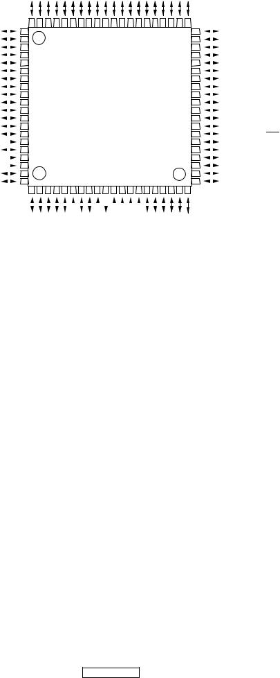
NOTES: 1. P7_0 and P7_1 are N channel open-drain output pins.
M30621FJPFP Terminal Function
Pin |
Pin Function |
Pin Name |
I/O |
STBY |
STOP |
Active |
Function |
|
|
|
|
|
|
|
|
1 |
P95/CLK4 |
ICLK |
O |
O/L |
O/L |
|
E2PROM CLOCK |
2 |
P94/TB4 |
RDS_DO |
I |
I |
O/L |
Lv |
RDS decoder seial data input(LC72722) |
3 |
P93/TB3 |
RDS_CE |
O |
O/L |
O/L |
|
RDS decoder seial data Chip Enable(LC72722) |
4 |
P92/SOUT3 |
RDS_DI |
O |
O/L |
O/L |
|
RDS decoder seial data output(LC72722) |
5 |
P90/CLK3 |
RDS_CL |
O |
O/L |
O/L |
|
RDS decoder seial data CLOCK(LC72722) |
6 |
CNVCS(BYTE) |
CNVSS |
- |
- |
- |
|
UP GRADE PIN |
7 |
P87 |
FM_MUTE |
O |
O/L |
O/L |
H:ACTIVE |
FM/AM RADIO ANALOG MUTE |
8 |
P86 |
NA/EU_SEL |
O |
O/L |
O/L |
H:ACTIVE |
NORTH AMERICA/EUédå¸SELECT Lo:NA |
9 |
RESET |
HARD RST |
I |
I |
I |
Lv |
u-COM RESET SIGNAL INPUT |
10 |
XOUT |
XOUT |
O |
- |
- |
|
OSILATOR CONNECTION |
11 |
VSS |
Vss |
GND |
- |
- |
|
GND |
12 |
XIN |
XIN |
I |
I |
I |
|
OSILATOR CONNECTION |
13 |
VCC |
Vcc1 |
3.3V |
- |
- |
|
POWER 3.3V |
14 |
P85/NMI |
NMI |
I |
- |
- |
|
PULL-UP |
15 |
P84/INT2 |
NC |
O |
O/L |
O/L |
|
OPEN |
16 |
P83/INT1 |
NC |
O |
O/L |
O/L |
|
OPEN |
17 |
P82/INT0 |
RDS_SYR |
I |
I |
I |
H:ACTIVE |
RDS decoder SYNCH&RAM RESET(LC72722) |
18 |
P81 |
STERO |
I |
I |
I |
|
STEREO BROADCAST DETECT |
19 |
P80 |
TUNED |
O |
O/L |
O/L |
|
TUNEDE DETECT |
20 |
P77 |
NC |
O |
O/L |
O/L |
|
OPEN |
21 |
P76 |
NC |
O |
O/L |
O/L |
|
OPEN |
22 |
P71/RXD2 |
NC |
O |
O/L |
O/L |
|
OPEN |
23 |
P70/TXD2 |
NC |
O |
O/L |
O/L |
|
OPEN |
24 |
P67/TXD1 |
PLL_DT |
O |
O/L |
O/L |
UART |
FM/AM MODULECommunication control terminal TX |
25 |
P66/RXD1 |
PLL_DT_IN |
I |
I |
O/L |
UART |
FM/AM MODULECommunication control terminal RX |
26 |
P65/CLK1 |
PLL_CLK |
O |
O/H |
O/L |
|
FM/AM MODULECommunication control terminalCLOCK |
27 |
P64/CTS1 |
PLL_CS |
O |
O/L |
O/L |
Fall Edge&L |
FM/AM MODULECommunication control terminal CS |
22 TU-604CI
Loading...