


 Loading...
For U.K. model
SERVICE MANUAL |
Ver. 1 |
|
MODEL TU-1800DAB
AM-FM STEREO/DAB TUNER
●For purposes of improvement, specifications and design are subject to change without notice.
●Please use this service manual with referring to the operating instructions without fail.
●Some illustrations using in this service manual are slightly different from the actual set.
|
● ● 8
●
●
TOKYO JAPAN
Denon Brand Company, D&M Holdings Inc.
X0237 V.01 DE/CDM 0507
TU-1800DAB
SAFETY PRECAUTIONS
The following check should be performed for the continued protection of the customer and service technician.
LEAKAGE CURRENT CHECK
Before returning the unit to the customer, make sure you make either (1) a leakage current check or (2) a line to chassis resistance check. If the leakage current exceeds 0.5 milliamps, or if the resistance from chassis to either side of the power cord is less than 460 kohms, the unit is defective.
|
|
|
|
|
|
|
|
|
500 |
|
|
|
|
|
1 Ω |
|
|

(1)
(2)

さい。特に配線図、部品表に
|
|
|
|
|
|
|
|
|
|
|
|
|
|
|
|
|
|
|
|
|
|
|
|
|
|
|
(1) … |
|
|
|
(2) … |
|
|
||
|
|
|
|
|
|
|
|
|
|
|
|
2
TU-1800DAB
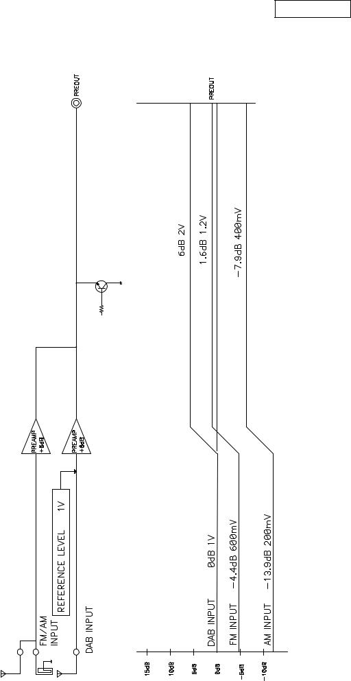
LEVEL DIAGRAMS
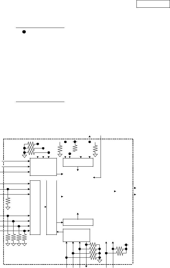
3

BLOCK DIAGRAMS
TU-1800DAB
4 |
TU-1800DAB
SEMICONDUCTORS
Only major semiconductors are shown, general semiconductors etc. are omitted to list.
1. IC’s
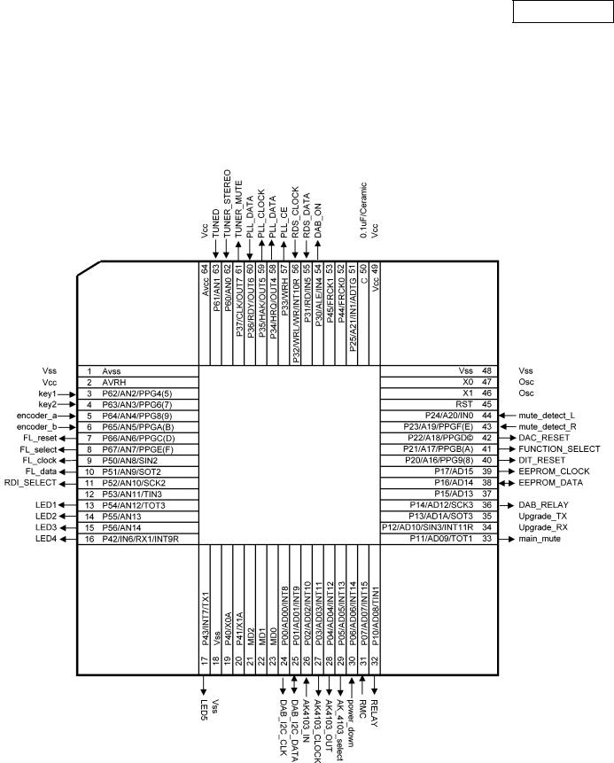
MB90F352C (IC300)
5
TU-1800DAB
MB90F352C Terminal Function
Pin No. |
Pin Name |
I/O |
Function |
|
|
|
|
|
|
|
|
1 |
Avss |
|
Vss |
2 |
AVRH |
|
Vcc |
3 |
P62/AN2/PPG4(5) |
I |
key1 |
4 |
P63/AN3/PPG6(7) |
I |
key2 |
5 |
P64/AN4/PPG8(9) |
I |
encoder_a |
6 |
P65/AN5/PPGA(B) |
I |
encoder_b |
7 |
P66/AN6/PPGC(D) |
O |
FLT_RESET |
8 |
P67/AN7/PPGE(F) |
O |
FLT_SELECT |
9 |
P50/AN8/SIN2 |
O |
FLT_CLOCK |
10 |
P51/AN9/SOT2 |
O |
FLT_DATA |
11 |
P52/AN10/SCK2 |
O |
RDI_SELECT |
12 |
P53/AN11/TIN3 |
O |
|
13 |
P54/AN12/TOT3 |
O |
LED_STANDBY |
14 |
P55/AN13 |
O |
LED_STEREO |
15 |
P56/AN14 |
O |
LED_SECONDARY |
16 |
P42/IN6/RX1/INT9R |
O |
LED_TUNED |
17 |
P43/INT7/TX1 |
O |
LED_RDS |
18 |
Vss |
|
GND |
19 |
P40/X0A |
|
|
20 |
P41/X1A |
|
|
21 |
MD2 |
|
MICOM UPGRADE |
22 |
MD1 |
|
MICOM UPGRADE |
23 |
MD0 |
|
MICOM UPGRADE |
24 |
P00/AD00/INT8 |
O |
DAB_I2C_CLOCK |
25 |
P01/AD01/INT9 |
O |
DAB_I2C_DATA |
26 |
P02/AD02/INT10 |
I |
AK4103_DATA_IN |
27 |
P03/AD03/INT11 |
O |
AK4103_CLOCK |
28 |
P04/AD04/INT12 |
O |
AK4103_DATA_OUT |
29 |
P05/AD05/INT13 |
O |
AK4103_SELECT |
30 |
P06/AD06/INT14 |
I |
POWER_DOWN |
31 |
P07/AD07/INT15 |
I |
REMOCON |
32 |
P10/AD08/TIN1 |
O |
POWER_RELAY |
33 |
P11/AD09/TOT1 |
O |
MAIN_MUTE |
34 |
P12/AD10/SIN3/INT11R |
O |
UPGRADE_RX |
35 |
P13/AD1A/SOT3 |
O |
UPGRADE_TX |
36 |
P14/AD12/SCK3 |
O |
POWER_DAB |
37 |
P15/AD13 |
O |
|
38 |
P16/AD14 |
O |
EEPROM_DATA |
39 |
P17/AD15 |
O |
EEPROM_CLOCK |
40 |
P20/A16/PPG9(8) |
O |
DIT_RESET |
41 |
P21/A17/PPGB(A) |
O |
FUNCTION_RELAY |
42 |
P22/A18/PPGD? |
O |
DAC_RESET |
43 |
P23/A19/PPGF(E) |
I |
DAC_MUTE_DETECT_R |
44 |
P24/A20/IN0 |
I |
DAC_MUTE_DETECT_L |
45 |
RST |
|
|
46 |
X1 |
|
4MHz |
47 |
X0 |
|
4MHz |
48 |
Vss |
|
|
49 |
Vcc |
|
|
50 |
C |
|
0.1UF/CERAMIC |
51 |
P25/A21/IN1/ADTG |
O |
DAC_MUTE |
52 |
P44/FRCK0 |
O |
|
53 |
P45/FRCK1 |
O |
|
54 |
P30/ALE/IN4 |
O |
DAB_ON |
55 |
P31/RD/IN5 |
I |
RDS_DATA |
56 |
P32/WRL/WR/INT10R |
I |
RDS_CLOCK |
57 |
P33/WRH |
O |
PLL_CE |
58 |
P34/HRQ/OUT4 |
O |
PLL_DATA_OUT(PLL DATA TRANS ) |
59 |
P35/HAK/OUT5 |
O |
PLL_CLOCK |
60 |
P36/RDY/OUT6 |
I |
PLL_DATA_IN(IF READ) |
61 |
P37/CLK/OUT7 |
O |
TUNER_MUTE |
62 |
P60/AN0 |
I |
TUNER_STEREO |
63 |
P61/AN1 |
I |
TUNER_TUNED |
64 |
Avcc |
|
VCC |
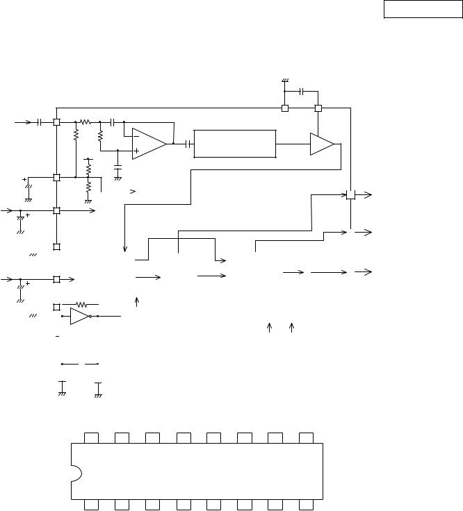
6
AK4103A (IC304)
V1 |
|
1 |
|
||
|
|
|
TRANS |
|
2 |
|
|
|
PDN |
|
3 |
|
|
|
|
|
|
MCLK |
|
4 |
|
|
|
|
|
|
SDTI |
|
5 |
|
|
|
BICK |
|
6 |
|
|
|
|
|
|
LRCK |
|
7 |
|
|
|
|
|
|
FS0/CSN |
|
8 |
|
|
|
FS1/CDTI |
|
9 |
|
|
|
|
|
|
FS2/CCLK |
|
10 |
|
|
|
|
|
|
FS3/CDTO |
|
11 |
|
|
|
|
|
|
C1 |
|
12 |
|
|
|
|
|
|
AK4103A BLOCK DIAGRAM
BICK 

LRCK 

SDTI
C1
U1
V1
FS0
FS1
FS2
FS3
TU-1800DAB
|
24 |
|
U1 |
|
|
||
|
23 |
|
DIF2 |
|
|
||
|
22 |
|
DIF1 |
|
|
||
|
21 |
|
DIF0 |
|
|
||
|
|
||
|
20 |
|
TXP |
|
|
||
|
|
||
Top |
19 |
|
TXN |
|
|||
|
|
|
|
View |
18 |
|
VSS |
|
|||
|
|
||
|
17 |
|
VDD |
|
|
||
|
|
||
|
16 |
|
CKS1 |
|
|
||
|
15 |
|
CKS0 |
|
|
||
|
|
||
|
14 |
|
BLS |
|
|
||
|
|
||
|
13 |
|
ANS |
|
|
||
|
|
||
|
|
|
|
|
|
|
|
DIF2 |
DIF1 |
DIF0 |
CKS1 |
CKS0 |
MCLK |
BLS |
TRANS |
VSS |
VDD |
|||||||
|
|
|
|
|
|
|
|
|
|
|
|
|
|
|
|
|
|
|
|
|
|
|
|
|
|
|
|
|
|
|
|
|
|
|
|
|
|
|
|
|
|
|
|
|
|
|
|
|
|
|
|
|
|
|
|
|
|
|
|
|
|
|
|
|
|
|
|
|
|
|
|
|
|
|
|
|
|
|
|
|
|
|
|
|
|
|
|
|
|
|
|
|
|
|
|
|
|
|
|
|
|
|
|
|
|
|
|
|
|
|
|
|
|
|
|
|
|
|
Prescaler
Audio Serial
Interface
|
|
|
|
|
|
|
|
|
|
Driver |
|
TXP |
|
|
|
|
|
|
|
|
|
|
|
||
|
|
|
|
|
|
|
Biphase |
|
|
Line |
|
|
|
|
|
|
|
|
|
|
|
|
|
||
|
|
|
|
|
|
|
Encoder |
|
|
|
TXN |
|
|
|
|
|
|
|
|
|
|
|
|||
|
|
|
|
|
|
|
|
|
RS422 |
|
||
MUX |
|
|
Register |
|
|
|
|
|
|
|
||
|
|
|
|
|
|
|
|
|
|
|||
|
|
|
|
|
|
|
|
|
|
CRCC Generator
Host Serial
Interface
CSN |
CCLK |
CDTI |
CDTO |
ANS |
PDN |
7

TU-1800DAB
AK4103A TERMINAL FUNCTION
No. |
Pin Name |
|
I/O |
|
|
|
|
|
Description |
|
|
|
||||||||||||
1 |
V1 |
|
|
I |
Validity Bit Input Pin |
|
|
|
||||||||||||||||
2 |
TRANS |
|
|
I |
Audio Routing Mode (Transparent Mode) Pin at Synchronous mode |
|||||||||||||||||||
|
|
|
|
|
|
|
|
|
|
|
|
|
0: Normal mode, 1: Audio routing mode (transparent mode) |
|||||||||||
3 |
PDN |
|
|
I |
Power Down & Reset Pin |
(Pull-up Pin) |
||||||||||||||||||
|
|
|
|
|
|
|
|
|
|
|
|
|
When “L”, the AK4103A is powered-down, TXP/N pins are “L” and the |
|||||||||||
|
|
|
|
|
|
|
|
|
|
|
|
|
control registers are reset to default values. |
|
|
|
||||||||
4 |
MCLK |
|
|
I |
Master Clock Input Pin |
|
|
|
||||||||||||||||
5 |
SDTI |
|
|
I |
Audio Serial Data Input Pin |
|
|
|
||||||||||||||||
6 |
BICK |
|
I/O |
Audio Serial Data Clock Input/Output Pin |
|
|
|
|||||||||||||||||
|
|
|
|
|
|
|
|
|
|
|
|
|
Serial Clock for SDTI pin which can be configured as an output based on |
|||||||||||
|
|
|
|
|
|
|
|
|
|
|
|
|
the DIF2-0 inputs. |
|
|
|
||||||||
7 |
LRCK |
|
I/O |
Input/Output Channel Clock Pin |
|
|
|
|||||||||||||||||
|
|
|
|
|
|
|
|
|
|
|
|
|
Indicates left or right channel, and can be configured as an output based on |
|||||||||||
|
|
|
|
|
|
|
|
|
|
|
|
|
the DIF2-0 inputs. |
|
|
|
||||||||
8 |
FS0 |
|
|
I |
Sampling Frequency Select 0 Pin at Synchronous mode (Pull-down Pin) |
|||||||||||||||||||
|
CSN |
|
|
I |
Host Interface Chip Select Pin at Asynchronous mode |
(Pull-down Pin) |
||||||||||||||||||
|
AKMODE |
|
|
I |
AK4112B Mode Pin at Audio routing mode |
(Pull-down Pin) |
||||||||||||||||||
|
|
|
|
|
|
|
|
|
|
|
|
|
0: Non-AKM receivers mode, 1: AK4112B mode |
|
|
|
||||||||
9 |
FS1 |
|
|
I |
Sampling Frequency Select 1 Pin at Synchronous mode (Pull-down Pin) |
|||||||||||||||||||
|
CDTI |
|
|
I |
Host Interface Data Input Pin at Asynchronous mode |
(Pull-down Pin) |
||||||||||||||||||
10 |
FS2 |
|
|
|
|
|
|
I |
|
|
Sampling Frequency Select 2 Pin at Synchronous mode (Pull-down Pin) |
|||||||||||||
|
|
|
|
|
|
|
|
|
|
|
|
|
|
|
|
|
|
|
|
|
|
|
|
|
|
CCLK |
|
|
|
|
|
|
I |
|
|
Host Interface Bit Clock Input Pin at Asynchronous mode (Pull-down Pin) |
|||||||||||||
11 |
FS3 |
|
|
|
|
|
|
I |
|
|
Sampling Frequency Select 3 Pin at Synchronous mode (Pull-down Pin) |
|||||||||||||
|
|
|
|
|
|
|
|
|
|
|
|
|
|
|
|
|
|
|
|
|
|
|
|
|
|
CDTO |
|
|
|
|
|
|
O |
|
|
Host Interface Data Output Pin at Asynchronous mode (Pull-down Pin) |
|||||||||||||
12 |
C1 |
|
|
I |
Channel Status Bit Input Pin |
|
|
|
||||||||||||||||
13 |
ANS |
|
|
I |
Asynchronous/Synchronous Mode Select Pin |
(Pull-up Pin) |
||||||||||||||||||
|
|
|
|
|
|
|
|
|
|
|
|
|
0: Asynchronous mode, 1: Synchronous mode |
|
|
|
||||||||
14 |
BLS |
|
I/O |
Block Start Input/Output Pin |
(Pull-down Pin) |
|||||||||||||||||||
|
|
|
|
|
|
|
|
|
|
|
|
|
In normal mode, the channel status block output is “H” for the first four |
|||||||||||
|
|
|
|
|
|
|
|
|
|
|
|
|
bytes. In audio routing mode, the pin is configured as an input. When PDN |
|||||||||||
|
|
|
|
|
|
|
|
|
|
|
|
|
pin = “L”, BLS pin goes “H” at Normal mode. |
|
|
|
||||||||
15 |
CKS0 |
|
|
I |
Clock Mode Select 0 Pin |
(Pull-up Pin) |
||||||||||||||||||
16 |
CKS1 |
|
|
I |
Clock Mode Select 1 Pin |
(Pull-down Pin) |
||||||||||||||||||
17 |
VDD |
- |
|
|
Power Supply Pin, 4.75V 5.25V |
|
|
|
||||||||||||||||
18 |
VSS |
- |
|
|
Ground Pin, 0V |
|
|
|
||||||||||||||||
19 |
TXN |
|
|
O |
Negative Differential Output Pin |
|
|
|
||||||||||||||||
20 |
TXP |
|
|
O |
Positive Differential Output Pin |
|
|
|
||||||||||||||||
21 |
DIF0 |
|
|
I |
Audio Serial Interface Select 0 Pin |
(Pull-down Pin) |
||||||||||||||||||
22 |
DIF1 |
|
|
I |
Audio Serial Interface Select 1 Pin |
(Pull-down Pin) |
||||||||||||||||||
23 |
DIF2 |
|
|
I |
Audio Serial Interface Select 2 Pin |
(Pull-down Pin) |
||||||||||||||||||
24 |
U1 |
|
|
I |
User Data Bit Input Pin for Channel 1 |
(Pull-down Pin) |
||||||||||||||||||
Notes:
1.Internal pull-up and pull-down resistors are connected on-chip. The value of the resistors is 43kΩ (typ).
2.All input pins except internal pull-down/pull-up pins should not be left floating.
8
TU-1800DAB
BU1924F (IC306)
|
|
|
|
|
|
560p |
|
|
|
|
|
|
CMP |
MUX |
(4) |
100k |
|
|
(7) |
(8) |
|
|
|
|
VSS3 |
|
|
270p |
120k |
|
|
|
|
|
|
100k |
|
|
|
|
|
|
|
8th |
Switched |
|
||
|
|
|
|
|||
|
|
|
capacitor |
filter |
|
|
|
|
|
anti-aliasing |
|
|
comparator |
|
|
|
|
|
|
|
Vref |
(3) |
|
filter |
|
|
|
 (16) RCLK 2.2 F

VDD1 (5)
1Analog
|
|
|
|
|
|
|
|
|
Power supply |
|
|
|
|
|
|
|
|
|
|
|
|
|
|
|
|
|
|
|
|
(1) QUAL |
||||||||
|
|
|
|
|
|
|
|
|
|
|
|
|
|
|
|
|
|
|
|
|
|
|
|
|
|
|
|
|
|
|
|
|
|
|
||||
|
|
|
VSS1 |
(6) |
|
|
|
|
|
|
|
|
|
|
|
|
|
|
|
|
|
|
|
|
|
|
|
|
|
|
|
|
|
|||||
|
|
|
|
|
|
|
|
|
|
|
|
|
|
|
|
|
|
|
|
|
|
|
|
|
|
|
|
|
|
|
|
|||||||
|
|
|
|
|
|
|
|
|
|
|
|
|
|
|
|
|
|
|
|
|
|
|
|
|
|
|
|
|
|
|
|
|||||||
|
|
|
|
|
|
|
|
|
|
|
|
|
|
|
|
|
|
|
|
|
|
|
|
|
|
|
|
|
|
|
|
|
|
|
|
|
|
RDATA |
|
|
|
|
|
|
|
|
|
|
|
|
|
|
|
|
|
|
|
|
|
|
|
|
|
|
|
|
|
|
|
|
|
|
|
|
|
|
|
|
|
|
|
|
|
|
|
|
|
|
|
|
|
|
|
|
PLL |
|
|
|
PLL |
|
|
Bi-phase |
|
|
|
|
Differential |
|
(2) |
|
||||||
|
|
|
|
|
|
|
|
|
|
|
|
|
|
|
|
|
57kHZ |
|
|
|
|
|
|
|
|
|
|
|
|
|||||||||
1 |
|
|
VDD2 |
|
|
(12) |
|
|
|
|
|
|
|
|
|
1187.5Hz |
|
decoder |
|
|
|
|
decoder |
|
|
|
|
|
||||||||||
|
|
|
|
|
|
|
|
|
|
RDS/ARI |
|
|
|
|
|
|
|
|
|
|
|
|
|
|||||||||||||||
|
|
|
|
|
|
|
|
|
|
|
|
|
|
|
|
|
|
|
|
|
|
|
|
|
|
|
||||||||||||
|
2 |
|
|
|
|
|
|
Digital |
|
|
|
|
|
|
|
|
|
|
|
|
|
|
|
|
|
|
|
|
|
|
|
|
||||||
|
|
|
|
|
|
|
Power supply |
|
|
|
|
|
|
|
|
|
|
|
|
|
|
|
|
|
|
|
|
|
|
|
|
|||||||
|
|
|
VSS2 |
|
|
(11) |
|
|
|
|
|
|
|
|
|
|
|
|
|
|
|
|
|
|
|
|
|
|
|
|
|
|
|
|
||||
|
|
|
|
|
|
|
|
|
|
|
|
|
|
|
|
|
|
|
|
|
|
|
|
|
|
|
|
|
||||||||||
|
|
|
|
|
|
|
|
|
|
|
|
|
|
|
|
|
|
|
|
|
|
|
|
|
|
|
|
|
|
|
|
|
|
|
|
|
|
|
|
|
|
|
|
|
|
|
|
|
|
|
|
|
|
|
|
|
|
|
|
|
|
|
|
|
|
|
|
|
|
|
|
|
|
|
|
|
|
|
|
|
|
|
|
|
|
|
|
|
|
|
|
|
|
|
|
|
Reference |
|
|
|
|
|
Measurement |
|
|
|
|
|
|
|
|
|||||
|
|
|
|
|
|
|
|
|
|
|
|
|
|
|
|
|
|
|
|
|
|
|
|
|
circuit |
|
|
|
|
|
|
|
|
|||||
|
|
|
|
|
|
|
|
|
|
|
|
|
|
|
|
|
|
|
clock |
|
|
|
|
|
|
|
|
|
|
|
|
|
|
|
||||
|
|
|
|
|
|
|
|
|
|
|
|
|
|
|
|
|
|
|
|
|
|
|
|
|
|
|
|
|
|
|
|
|
|
|
|
|||
|
|
|
|
|
|
|
|
|
|
(13) |
|
|
|
|
|
|
(14) |
|
|
|
|
|
|
|
(10) |
|
|
|
|
(9) |
|
|
|
|
|
|
||
|
|
|
|
|
|
|
|
|
|
|
|
|
|
|
|
|
|
|
|
|
|
|
|
|
|
|
|
|
|
|
|
|
||||||
|
|
|
|
XI |
|
|
|
|
|
|
|
|
|
XO |
|
|
|
|
|
|
|
|
|
|
|
|
T2 |
|
|
|
|
|||||||
|
|
|
|
|
|
|
|
|
|
|
|
|
|
|
|
|
|
|
|
|
|
|
|
|
|
T1 |
|
|
|
|
||||||||
|
|
|
|
|
|
|
|
|
|
4.332MHZ |
|
|
|
|
|
|
|
|
|
|
|
|
|
|
|
|
|
|
|
|
|
|
|
|
||||
|
|
|
|
|
|
|
|
|
|
|
|
|
|
|
|
|
|
|
|
|
|
|
1 : VDD1 and VDD2 are separated within the IC. |
|
|
|
|
|
|
|
|
|||||||
|
|
|
|
|
|
|
|
|
|
|
|
|
|
|
|
|
|
|
|
|
|
|
|
|
|
|
|
|
|
|
||||||||
|
|
|
|
33pF |
|
|
|
|
|
|
|
|
33pF |
|
|
|
|
2 : Have VDD2 (digital power supply) of a sufficiently low impedance. |
|
|
||||||||||||||||||
|
|
|
|
|
|
|
|
|
|
|
|
|
|
|
|
|
|
|||||||||||||||||||||
|
|
|
|
|
|
|
|
|
|
|
|
|
|
|
|
3 : Match the capacitor constants with the crystal manufacturer. |
|
|
|
|
||||||||||||||||||
|
|
|
|
|
|
|
|
|
|
|
|
|
|
|
|
|
|
|
|
|
|
|
|
|
|
|
||||||||||||
33
RCLK |
(N.C.) |
XO |
XI |
16 |
15 |
14 |
13 |
VDD2 |
VSS2 |
T1 |
12 |
11 |
10 |
T2 9
1
QUAL
2 |
3 |
4 |
RDATA |
Vref |
MUX |
5 |
6 |
7 |
VDD1 |
VSS1 |
VSS3 |
8 CMP
9
TU-1800DAB
M24C32 (IC704)
E0 |
1 |
8 |
VCC |
|
E1 |
2 |
7 |
WC |
|
E2 |
3 |
6 |
SCL |
|
VSS |
4 |
5 |
SDA |
|
BLOCK DIAGRAM
WC |
|
|
E0 |
High Voltage |
|
Control Logic |
Generator |
|
E1 |
||
|
||
E2 |
|
|
SCL |
|
|
SDA |
I/O Shift Register |
|
Address Register |
Data |
|
and Counter |
Register |
Y Decoder |
1 Page |
X Decoder |
SP8K5TB (IC105)
(8) |
(7) |
(6) |
(5) |
(8) |
(7) |
(6) |
(5) |
||||||||
|
|
|
|
|
|
|
|
|
|
|
|
|
|
|
|
|
|
|
|
|
|
|
|
|
|
|
|
|
|
|
|
2 |
|
2 |
(1) |
(2) |
(3) |
(4) |
||
|
|
|
||||||
|
|
|
|
(1) |
Tr1 Source |
|||
|
1 |
1 |
|
(2) |
Tr1 Gate |
|||
|
|
(3) |
Tr2 Source |
|||||
|
|
|
|
|||||
|
|
|
|
(4) |
Tr2 Gate |
|||
(1) |
(2) |
(3) |
(4) |
(5) |
Tr2 Drain |
|||
(6) |
Tr2 Drain |
|||||||
|
|
|
|
|||||
1 ESD PROTECTION DIODE |
|
(7) |
Tr1 Drain |
|||||
|
|
|
|
|
||||
2 BODY DIODE |
|
|
(8) |
Tr1 Drain |
||||
|
|
|
|
|
|
|||
10
Loading...