


Copyright and Warranty Notice
The information in this document is subject to change without notice and does not represent a commitment on part of the vendor, who assumes no liability or responsibility for any errors that may appear in this manual.
No warranty or representation, either expressed or implied, is made with respect to the quality, accuracy or fitness for any particular part of this document. In no event shall the manufacturer be liable for direct, indirect, special, incidental or consequential damages arising from any defect or error in this manual or product.
Product names appearing in this manual are for identification purpose only and trademarks and product names or brand names appearing in this document are property of their respective owners.
This document contains materials protected under International Copyright Laws. All rights reserved. No part of this manual may be reproduced, transmitted or transcribed without the expressed written permission of the manufacturer and authors of this manual.
If you do not properly set the motherboard settings causing the motherboard to malfunction or fail, we cannot guarantee any responsibility.


BE6 Motherboard User’s Manual
Table of Contents |
|
CHAPTER 1. INTRODUCTION OF BE6 FEATURES |
1-1 |
1-1.Features of This Motherboard |
1-1 |
1-2. Specifications |
1-2 |
1-3. Layout Diagram |
1-3 |
1-4. The System Block Diagram |
1-5 |
CHAPTER 2. INSTALLING THE MOTHERBOARD |
2-1 |
2-1. Installing the Motherboard to the Chassis |
2-2 |
2-2. Installation of the Pentium II/III, Celeron CPU |
2-3 |
2-3. Installing System Memory |
2-3 |
2-4. Connectors, Headers and Switches |
2-6 |
CHAPTER 3. INTRODUCTION OF THE BIOS |
3-1 |
3-1. CPU Setup [SOFT MENU™ II] |
3-3 |
3-2. Standard CMOS Setup Menu |
3-8 |
3-3. BIOS Features Setup Menu |
3-11 |
3-4. Chipset Features Setup Menu |
3-17 |
3-5. Power Management Setup Menu |
3-21 |
3-6. PNP/PCI Configuration |
3-28 |
3-7. Load Setup Defaults |
3-30 |
3-8. Integrated Peripherals |
3-31 |
3-9. Password Setting |
3-36 |
3-10. IDE Hard Disk Detection |
3-37 |
3-11. Save & Exit Setup |
3-38 |
3-12. Quit Without Saving |
3-38 |
APPENDIX A BIOS FLASHING USER INSTRUCTIONS
APPENDIX B INSTALLING THE HIGHPOINT XSTORE PRO UTILITY
APPENDIX C HARDWARE MONITORING FUNCTION (INSTALLING THE WINBOND HARDWARE DOCTOR UTILITY)
APPENDIX D INSTALLING THE DRIVER FOR ULTRA ATA/66 APPENDIX E THE THERMAL CABLE
APPENDIX F TROUBLESHOOTING (NEED ASSISTANCE?)
MN-163-2A1-71 |
Rev. 1.01 |


Introduction of BE6 Features |
1-1 |
|
|
Chapter 1. Introduction of BE6 Features
1-1.Features of This Motherboard
The motherboard is designed for a new generation CPUs. It supports the Intel SLOT1 structure (Pentium II/III and Celeron processors), up to 768MB of memory, super I/O, and Green PC functions. The motherboard provides high performance for server systems and meets the requirements for desktop system for multimedia in the future.
The BE6 has the HPT366 Ultra ATA/66 Chipset built-in. This means, the BE6 will support Ultra ATA/66 IDE devices. Ultra ATA/66 is the new standard for IDE devices. It enhances existing Ultra ATA/33 technology by increasing both performance and data integrity. This new high-speed interface doubles the Ultra ATA/33 burst data transfer rate to 66.6 Mbytes/sec. The result is maximum disc performance using the current PCI local bus environment. Another benefit is, you can connect another four IDE devices in your system either Ultra ATA/33 IDE devices or Ultra ATA/66 IDE devices. You will have more flexibility to expand your computer system.
The BE6 has built-in hardware monitoring functions (you can refer to Appendix C for detailed information), they can monitor and protect your computer insuring a safe computing environment. The BE6 also supports both the PS/2 keyboard and PS/2 mouse wake up features (you can refer to section 3-8 for detailed information), letting you easily wake up your system by these devices. The motherboard can provide high performance for workstations and meets the requirements for desktop systems for multimedia in the future.
Sets You Free From the Y2K Threat
The potential threat of Year 2000 (Y2K) problems are making everyone very nervous. The Y2K issue applies to almost any device, firmware, or software that operates on or with year based dates. This problem is caused by a design flaw in the Real Time Clock (RTC) unit. The RTC only changes the last two digits of the year code, but not the century information. As a result, when it comes to 12:00 AM January 1, 2000 the RTC will switch from December 31 11:59 PM 1999 to 12:00 AM January 1 1900.
Y2K compliance deals with the date change over from 31 December 1999 to 1 January 2000, and with recording and reporting of all dates from the RTC including leap year dates. This motherboard is free from the Y2K problem because its BIOS are Y2K compliant.
User’s Manual

1-2 |
Chapter1 |
|
|
Please Note
If the operating system or application software cannot handle Year 2000 dates, you will still be facing the Y2K threat because it is not a hardware problem that relates to the motherboard itself. According to Award BIOS, it is BIOS source code released after 31 May 1995 complies with all known Y2K issues; however, it may still fail the 2000.exe test. Award has modified its BIOS source code to accommodate the requirements of 2000.exe. Award BIOS source code issued later than 18 November 1996 passes the NTSL 2000.exe test program.
1-2. Specifications
1. CPU
! Supports Intel Pentium III 450 ~ 550 MHz Processor cartridge.
! Supports Intel Pentium II 233 ~ 450 MHz Processor cartridge.
! Supports Intel® Celeron™ 266 ~ 466MHz processors (Based on 66MHz PPGA package)
! Supports 66 and 100MHz CPU external clock speeds
2. Chipset
!Intel® 440BX chipset (82443BX and 82371EB)
!HPT366 Ultra DMA66 IDE controller supports four Ultra DMA66 devices
!Supports Ultra DMA/33 IDE protocol
!Supports Advanced Configuration and Power Management Interface (ACPI)
!Accelerated Graphics Port connector supports AGP 1x and 2x mode (Sideband) 3.3V device
3. Memory (System Memory)
! Three 168-pin DIMM sockets support SDRAM modules
! Supports up to 768MB MAX. (8, 16, 32, 64, 128, 256 MB SDRAM)
! Supports ECC
4. System BIOS
! CPU SOFT MENU™ II, can easily set the processor parameters
! AWARD BIOS
! Supports Plug-and-Play (PnP)
! Supports Advanced Configuration Power Interface (ACPI)
! Supports Desktop Management Interface (DMI)
! Year 2000 compliant
BE6

Introduction of BE6 Features |
1-3 |
|
|
5. Multi I/O Functions
!2x Channels of Bus Master IDE Ports supporting up to four Ultra DMA 33/66 devices
!2x Channels of Bus Master IDE Ports supporting up to four Ultra DMA 33 devices
!PS/2 Keyboard and PS/2 Mouse Connectors
!1x Floppy Port ( up to 2.88MB)
!1x Parallel Port (EPP/ECP)
!2x Serial Ports
!2x USB Connectors
6. Miscellaneous
!ATX form factor
!One AGP slot, five PCI slots and two ISA slots
!Supports PS/2 keyboard and PS/2 mouse wake-up functions
!Built-in Wake on LAN header
!Built-in IrDA TX/RX header
!Built-in SB-Link™ header
!Built-in Wake On Ring header
!Built-in SMBus header
!Hardware monitoring Included fan speed, voltages, CPU and system environment temperature
!One Thermal Sensor Cable included
!Board size: 305 * 210mm
User’s Manual
1-4 |
Chapter1 |
|
|
"Supports Wake On LAN, Keyboard or Mouse, but your ATX power supply 5V standby power must be able to provide at least a 720mA current capacity. Otherwise, the functions may not work normally.
"PCI slots 4 and 5 use the same bus master control signal.
"PCI slot 3 shares IRQ signals with the HPT366 IDE controller (Ultra ATA/66). The driver for HPT 366 IDE controller supports IRQ sharing with other PCI devices. But if you install a PCI card that doesn’t allow IRQ sharing with other devices into PCI slot 3, you may encounter some problems. Furthermore, if your Operating System doesn’t allow peripheral devices to share IRQ signals with each other-- Windows NT for example, you can’t install a PCI card into PCI slot 3.
"HPT 366 IDE controller is designed to support high-speed mass storage. Thus we don’t suggest you connect non-disk devices that use ATA/ATAPI interfaces, such as
CD-ROM to HPT 366 IDE connector (IDE3&IDE4).
#Above 66MHz/100MHz bus speeds are supported but not guaranteed due to the PCI and chipset specifications.
#Sound Blaster™ is a registered trademark of Creative Technology Ltd. in the United States and certain other countries. Sound Blaster - LINK™ and SB-LINK™ are trademarks of Creative Technology Ltd.
#Specifications and information contained in this manual are subject to change without notice.
Note
All brand names and trademarks are the property of their respective owners.
BE6
Introduction of BE6 Features |
1-5 |
|
|
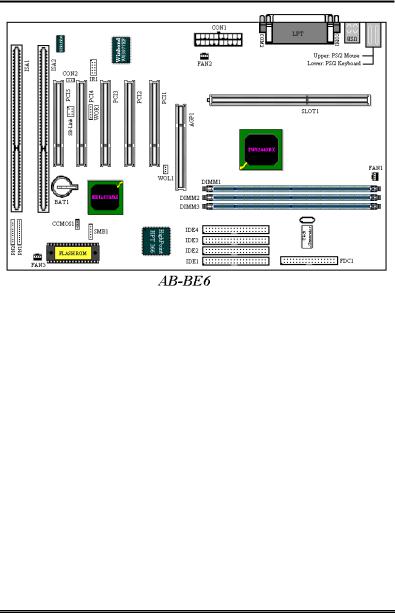
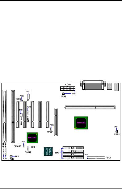
1-3. Layout Diagram
Figure 1-2. Motherboard component location
User’s Manual
1-6 |
Chapter1 |
|
|
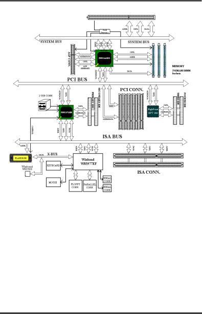
1-4. The System Block Diagram
Figure 1-3. System diagram of the 440BX chipset
BE6
Installing the Motherboard |
2-1 |
|
|
Chapter 2. Installing the Motherboard
This BE6 motherboard not only provides all standard equipment for classic personal computers, but also provides great flexibility for meeting future upgrade demands. This chapter will introduce step by step all the standard equipment and will also present, as completely as possible, future upgrade capabilities. This motherboard is able to support all Intel Pentium II/III processors and Intel Celeron processor now on the market. (For details, see specifications in Chapter 1.)
This chapter is organized according the following features:
2-1 Installing the Motherboard to the Chassis
2-2 Installation of the Pentium II/III, Celeron CPU 2-3 Installing System Memory
2-4 Connectors, Headers and Switches
$$$$ Before Proceeding with the Installation $$$$
Before you install or unplug any connectors or add-on cards, please remember to turn the ATX power supply switch off (fully turn the +5V standby power off), or take the power cord off. Otherwise, you may cause the motherboard components or add-on cards to malfunction or be damaged.
%
User Friendly Instructions
Our objective is to enable the novice computer user to perform the installation by himself. We have attempted to write this document in a very clear, concise and descriptive manner to help overcome any obstacles you may face during installation. Please read our instructions carefully and follow them step-by-step.
User’s Manual
2-2 |
Chapter2 |
|
|
2-1. Installing the Motherboard to the Chassis
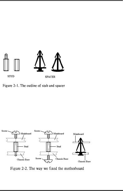
Most computer chassis will have a base on which there will be many mounting holes that allows the motherboard to be securely attached and at the same time, prevents short circuits. There are two ways to attach the motherboard to the base of chassis:
!with studs
!or with spacers
Please refer to the figure 2-1 that shows the studs and spacers, they may have several types, but all look like the figures below:
In principle, the best way to attach the motherboard is with studs, and only if you are unable to do this should you attach the board with spacers. Take a careful look at the motherboard and you will see many mounting holes on it. Line these holes up with the mounting holes on the base. If the holes line up, and there are screw holes
this means you can attach the motherboard with studs. If the holes line up and there are only slots, this means you can only attach the motherboard with spacers. Take the tip of the spacers and insert them into the slots. After doing this to all the slots, you can slide the motherboard into position aligned with the slots. After the motherboard has been positioned, check to make sure everything is OK before putting the casing back on.
Figure 2-2 shows you the way to affix the motherboard using studs or spacers:
BE6
Installing the Motherboard |
2-3 |
|
|
Note
If the motherboard has mounting holes, but they don’t line up with the holes on the base and there are no slots to attach the spacers, don’t worry, you can still attach the spacers to the mounting holes. Just cut the bottom portion of spacers (the spacer may be a little hard to cut off, so be careful of your hands). In this way you can still attach the motherboard to the base without worrying about short circuits. Sometimes you may need to use the plastic springs to isolate the screw from the motherboard PCB surface, because the circuit wire may be near by the hole. Be careful, don’t let the screw contact any printed circuit wire or parts on the PCB that are near the fixing hole, otherwise it may damage the board or cause board malfunctioning.
2-2. Installation of the Pentium II/III, Celeron CPU
The installation method for the CPU is printed on the package of the retention mechanism that comes with the motherboard. You can refer to it while you install the CPU. This motherboard also supports the Celeron® PPGA processor. If you want to install the Celeron® PPGA processor, you have to use an additional adapter that allows you to use a Celeron® PPGA processor in a slot 1 board. For this ABIT makes the SlotKET adapter.
Note:
!Installing a heat sink and cooling fan is necessary for proper heat dissipation from your CPU. Failing to install these items may result in overheating and damage of your CPU.
!Please refer to your boxed processor installation or other documentation attached with your CPU for detailed installing instructions.
2-3. Installing System Memory
This motherboard provides three 168-pin DIMM sites for memory expansion. The DIMM sockets support 1Mx64 (8MB), 2Mx64 (16MB), 4Mx64 (32MB), 8Mx64 (64MB), 16Mx64 (128MB), and 32Mx64 (256MB) or double sided DIMM modules. Minimum memory size is 8MB and maximum memory size is 768MB SDRAM. There are three Memory module sockets on the system board. (Total six banks)
User’s Manual
2-4 |
Chapter2 |
|
|
In order to create a memory array, certain rules must be followed. The following set of rules
allows for optimum configurations.
!The memory array is 64 or 72 bits wide. (depending on with or without parity)
!Those modules can be populated in any order.
!Supports single and double density DIMMS.
Table 2-1. Valid Memory Configurations
Bank |
|
Memory Module |
Total Memory |
|
|
|
|
Bank 0, 1 |
|
8MB, 16MB, 32MB, |
8MB ~ 256MB |
(DIMM1) |
|
64MB, 128MB, 256MB |
|
|
|
||
Bank 2, 3 |
|
8MB, 16MB, 32MB, |
8MB ~ 256MB |
(DIMM2) |
|
64MB, 128MB, 256MB |
|
|
|
||
Bank 4, 5 |
|
8MB, 16MB, 32MB, |
8MB ~ 256MB |
(DIMM3) |
|
64MB, 128MB, 256MB |
|
|
|
||
Total System Memory |
|
8MB ~ 768MB |
|
|
|
|
|
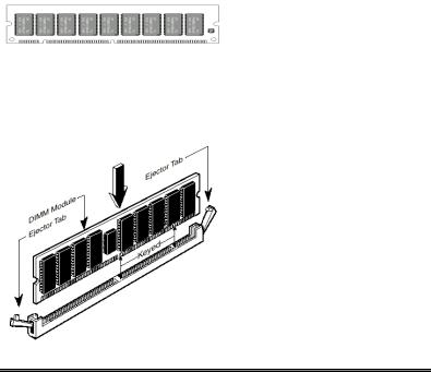
Generally, installing SDRAM modules to your motherboard is an easy thing to do. You can refer to figure 2-3 to see what a 168-pin PC100 SDRAM module looks like.
Unlike installing SIMMs, DIMMs may be "snapped" directly into the socket. Note: Certain DIMM sockets have minor physical differences. If your module
doesn't seem to fit, please do not force it into the socket as you may damaged your memory module or DIMM socket.
The following procedure will show you how to install a DIMM module into a DIMM socket.
Step 1. Before you install the memory module, please place the computer power switch in the off position and disconnect the AC power cord from your computer.
Step 2. Remove the computer’s chassis
cover.
Step 3. Before touching any electronic components, make sure you first touch an unpainted, grounded metal object to discharge any static electricity stored on
your clothing or body.
Figure 2-4. Memory module installation
BE6

Installing the Motherboard |
2-5 |
|
|
Step 4. Locate your computer’s 168-pin memory expansion DIMM socket.
Step 5. Insert the DIMM module into the expansion socket as shown in the illustration. Note how the module is keyed to the socket. You can refer to figure 2-4 for the details. This insures the DIMM module will be plugged into the socket in one way only. Firmly press the DIMM module into the DIMM socket, making certain the module is completely seated in the DIMM socket.
Step 6. Once the DIMM module has been installed, the installation is complete and the computer’s cover can be replaced. Or you can continue to install other devices and add-on cards that are mentioned in the following section.
Note
When you install a DIMM module fully into the DIMM socket, the eject tab should be locked into the DIMM module very firmly and fit into its indention on the both sides.
User’s Manual
2-6 |
Chapter2 |
|
|
2-4. Connectors, Headers and Switches
Inside the case of any computer several cables and plugs have to be connected. These cables and plugs are usually connected one-by-one to connectors located on the motherboard. You need to carefully pay attention to any connection orientation the cables may have and, if any, notice the position of the first pin of the connector. In the explanations that follow, we will describe the significance of the first pin.
We will show you all connectors, headers and switches here, and tell you how to connect them. Please pay attention and read the whole section for necessary information before attempting to finish all of the hardware installation inside the computer chassis.
Figure 2-5 shows you all of the connectors and headers that we’ll discuss in the next section, you can use this diagram to visually locate each connector and header we describe.
All connectors, headers and switches mentioned here, will depend on your system configuration. Some features you may (or may not) have and need to connect or configure depending on the peripheral. If your system doesn't have such add-on cards or switches you can ignore some special feature connectors.
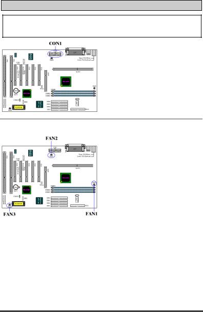
Figure 2-5. All Connectors and Headers for the BE6
First, Let’s see the headers that BE6 uses, and what their functions are.
BE6
Installing the Motherboard |
2-7 |
|
|
|
|
CON1: ATX Power Input Connector
Caution
If the power supply connectors are not properly attached to the CON1 power supply, the power supply or add-on cards may be damaged.
Attach the connector from the power supply to the CON1 connector here. Remember you have to push the connector from the ATX power supply firmly to the end with the CON1 connector, insuring that you have a good connection.
Note: Watch the pin position and the orientation
FAN1, FAN2 & FAN3: FAN header
Attach the connector from the individual CPU fan to the header named FAN2, and attach the connector from the chassis fan to FAN1 or & FAN3 header.
You must attach the CPU fan to the processor, or your processor will work abnormally or may be damaged by overheating. Also, if you want the computer case’s internal temperature to be kept steady and not too high, you had better connect the chassis fan to reach this goal.
Note: Watch the pin position and the orientation
User’s Manual
2-8 |
Chapter2 |
|
|
|
|
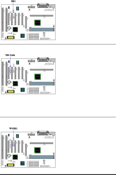
IR1: IR Header (Infrared) |
|
|
There is a specific orientation for pins 1 |
|
through 5, attach the connector from the IR |
|
KIT or IR device to the IR1 header (left row |
|
only) This motherboard supports standard |
|
IR transfer rates. |
|
Note: Watch the pin position and the |
|
orientation |
SB-Link: SB-Link™ Header
If your PCI audio adapter supports this feature, then you can connect the specific cable from the audio adapter to this header. SB-LINK™ combines Intel's PC-PCI and "Serialized IRQ" protocols. These technologies can be found in Intel's TX, LX, BX and newer core logic chipsets. This technology provides the DMA and IRQ signals present in ISA Bus today, but not available on the PCI Bus. The SB-LINK™
serves as a bridge between the motherboard and PCI sound card to deliver Sound card for real-mode DOS games. Check to see if your card supports this.
Note: Watch the pin position and the orientation
WOR1: Wake On Ring Header
If you have an internal modem adapter that supports this feature, then you can connect the specific cable from the internal modem adapter to this header. This feature lets you wake up your computer via remote control through the modem.
Note: Watch the pin position and the orientation
BE6
Installing the Motherboard |
2-9 |
|
|
|
|
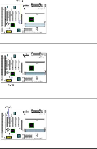
WOL1: Wake on LAN Header
If you have a Network adapter that supports this feature, then you can connect the specific cable from the network adapter to this header. This feature lets you wake up your computer via remote control through a local area network. You may need a specific utility to control the wake up event, like using the Intel® LDCM® utility or other similar utilities.
Note: Watch the pin position and the orientation
SMB1: System Management Bus Connector
This connector is reserved for system management bus (SMBus). The SMBus is a specific implementation of an I2C bus. I2C is a multi-master bus, which means that multiple chips can be connected to the same bus and each one can act as a master by initiating a data transfer. If more than one master simultaneously tries to control the bus, an arbitration procedure decides which
master gets priority.
Note: Watch the pin position and the orientation
CON2 header:
This header is for you to connect an additional thermistor to detect the CPU temperature. You can attach one end of the two-threaded thermal cable that comes with the motherboard to CON2 header, then tape the other end of thermal cable on CPU’s heat sink.
Generally speaking, the location you tape the thermistor should be as near the CPU
chipset as possible and avoid having it near the CPU FAN.
User’s Manual
2-10 |
Chapter2 |
|
|
|
|
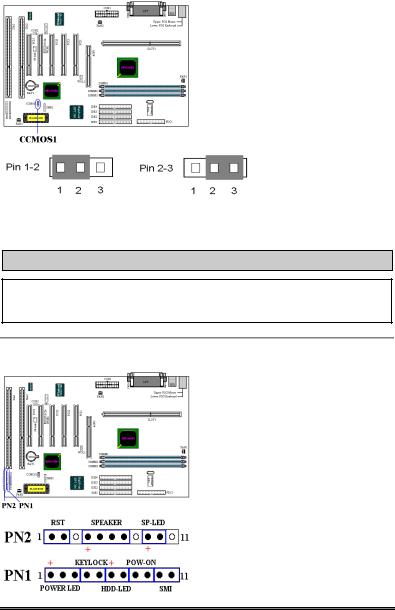
CCMOS1: CMOS Discharge Jumper
Jumper CCMOS1 discharge CMOS memory. When you install the motherboard, make sure this jumper is set for normal operation (pin 1 and 2 shorted). See figure 2-6.
Normal Operation (Default) |
Discharge CMOS |
Figure 2-6. CCMOS1 jumper setting
Note
Before you clear the CMOS, you have to turn the power off first (including the +5V standby power). Otherwise, your system may work abnormally or malfunction.
PN1 and PN2 Headers
PN1 and PN2 are for switches and indicators for the chassis’s front panel, there are several functions that come from these two headers. You have to watch the pin position and the orientation, or you may cause system malfunctions. Figure 2-7 shows you the PN1 and PN2 functions of the pins.
Figure 2-7. The definition of PN1 and
PN2 pins
BE6
Installing the Motherboard |
2-11 |
|
|
PN1 (Pin 1-2-3-4-5): Power LED and Keylock Switch Headers
There is a specific orientation for pins 1 through 3. Insert the three-threaded power LED cable to pins 1~3, and the two-threaded keylock cable into pin 4 and pin 5. Check to make sure the correct pins go to the correct connectors on the motherboard. If you
install them with the wrong direction, the power LED light will not illuminate correctly.
Note: Watch the power LED pin position and orientation.
PN1 (Pin 6-7): HDD LED Header
Attach the cable from the case’s front panel HDD LED to this header. If you install it in the wrong direction, the LED light will not illuminate correctly.
Note: Watch the HDD LED pin position and the orientation.
PN1 (Pin 8-9): Power on Switch Header
Attach the cable from the case’s front panel power switch to this header.
PN1 (Pin 10-11): Hardware Suspend Switch (SMI Switch) Header
Attach the cable from the case’s front panel suspend switch (if there is one) to this header. Use this switch to enable/disable the power management function by hardware.
Note: If you enable the ACPI function in the BIOS setup, this function will not work.
User’s Manual
2-12 |
Chapter2 |
|
|
|
|
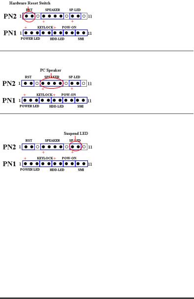
PN2 (Pin 1-2): Hardware Reset Switch Header
Attach the cable from the case’s front panel Reset switch to this header. Press and hold the reset button for at least one second to reset the system.
PN2 (Pin 4-5-6-7): Speaker Header
Attach the cable from the system speaker to this header.
PN2 (Pin 9-10): Suspend LED Header
Insert the two-threaded suspend LED cable into pin 9 and pin 10. If you install it in the wrong direction, the LED light will not illuminate correctly.
Note: Watch the HDD LED pin position and the orientation.
For the PN1 and PN2 pin’s count-name list, please refer to table 2-2.
BE6
|
Installing the Motherboard |
|
|
2-13 |
||
|
|
|
|
|
|
|
|
|
|
Table 2-2. PN1 and PN2 pin count name list |
|||
|
|
|
|
|
|
|
|
PIN Name |
Significance of signal |
PIN Name |
Significance of signal |
||
|
|
PIN 1 |
+5VDC |
|
PIN 1 |
Ground |
|
|
|
|
|
|
|
|
|
PIN 2 |
No connection |
|
PIN 2 |
Reset input |
|
|
PIN 3 |
Ground |
|
PIN 3 |
No connection |
|
|
PIN 4 |
Keyboard inhibit Signal |
|
PIN 4 |
+5VDC |
|
PN1 |
PIN 5 |
Ground |
PN2 |
PIN 5 |
Ground |
|
PIN6 |
LED power |
PIN6 |
Ground |
||
|
|
|
||||
|
|
PIN 7 |
HDD active |
|
PIN 7 |
Speaker data |
|
|
PIN 8 |
Ground |
|
PIN 8 |
No connection |
|
|
PIN 9 |
Power On/Off signal |
|
PIN 9 |
+5VDC |
|
|
PIN 10 |
+3V Standby |
|
PIN 10 |
Suspend LED active |
|
|
PIN 11 |
Suspend signal |
|
PIN 11 |
No connection |
Let’s now see the I/O connectors that BE6 uses, and what their functions are.
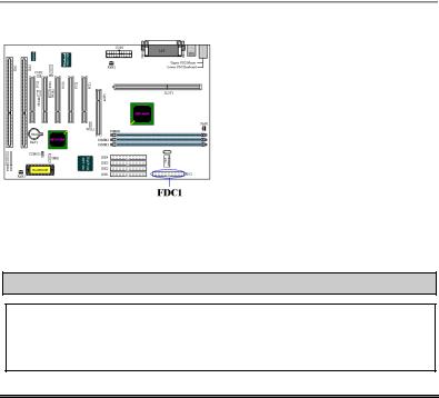
FDC1 Connector
This 34-pin connector is called the “floppy disk drive connector”. You can connect a 360K, 5.25”, 1.2M, 5.25”, 720K, 3.5’’, 1.44M, 3.5” or 2.88M, 3.5” floppy disk drive, you can even connect a 3 Mode floppy disk drive (it’s a 3 1/2” drive used in Japanese computer systems).
A floppy disk drive ribbon cable has 34 wires and two connectors to provide for the connection of two floppy disk drives. After connecting the single end to the FDC1, connect
the two connectors on the other end to the floppy disk drives. In general, people only install one floppy disk drive on their computer system.
Note
A red mark on a wire typically designates the location of pin 1. You need to align the wire pin 1 to the FDC1 connector pin 1, then insert the wire connector into the FDC1 connector.
User’s Manual
2-14 |
Chapter2 |
|
|
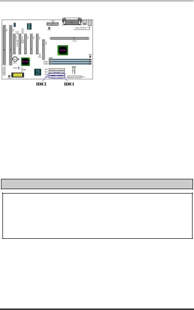
IDE1 and IDE2 Connectors
An IDE hard disk drive ribbon cable has 40 wires and two connectors to provide a connection for two IDE hard disk drives. After connecting the single end to the IDE1 (or IDE2), connect the two connectors on the other end to the IDE hard disk drives (or CD-ROM drive, LS-120, etc.).
Before you install a hard disk, there are some things you need to be aware of:
♦“Primary” refers to the first connector on the motherboard, that is, the IDE1 connector on the motherboard.
♦“Secondary” refers to the second connector on the motherboard, that is, the IDE2 connector on the motherboard.
♦Two hard disks can be connected to each connector: The first HDD is referred to as the “Master”,
The second HDD is referred to as the “Slave”.
♦For performance issues, we strongly suggest you don’t install a CD-ROM drive on the same IDE channel as a hard disk. Otherwise, the system performance on this channel may drop. (how much depends on your CD-ROM drive performance)
Note
!The Master or Slave status of the hard disk drive is set on the hard disk itself. Please refer to the hard disk drive user’s manual.
!A red mark on a wire typically designates the location of pin 1. You need to align the wire pin 1 to the FDC1 connector pin 1, then insert the wire connector into the FDC1 connector.
BE6

Installing the Motherboard |
2-15 |
|
|
IDE3 and IDE4: ATA 66/Connectors
The BE6 supports the Ultra ATA/66 (Also known as Ultra DMA/66) specification. It enhances existing Ultra ATA/33 technology by increasing both performance and data integrity. This new high-speed interface doubles the Ultra ATA/33 burst data transfer rate to 66.6 Mbytes/sec. The result is maximum disc performance using the current PCI local bus environment. Figure
2-8 shows you the different between the Ultra ATA/33 and Ultra ATA/66 Conductor Cable.
NOTE
HPT 366 IDE controller is designed to support high-speed mass storage. Thus we don’t suggest you connect non-disk devices that use ATA/ATAPI interfaces, such as CD-ROM to HPT 366 IDE connector (IDE3&IDE4).
Figure 2-8. The difference between Ultra ATA/33 and Ultra ATA/66 Conductor Cables
Figure 2-9 shows you a photo of an Ultra ATA/66 Conductor Cable. An Ultra ATA/66capable cable is a 40-pin, 80-conductor cable with a black connector on one end, a blue connector on the other end and a gray connector in the middle. In addition, line 34 on the cable should be notched or cut (this may be difficult to see).
Ultra ATA/66 is backwards compatible with all Ultra ATA/33 systems, but it will be limited in its transfer mode to the Ultra ATA/33 (Ultra DMA Mode 2 - 33 Mbytes/sec) or PIO Mode 4 (16.6 Mbytes/sec). Ultra ATA/66 hard drives are 100 percent backward compatible with both Ultra ATA/33 and DMA and with existing ATA (IDE) hard drives, CD-ROM drives,
User’s Manual
2-16 |
Chapter2 |
|
|
and host systems. The Ultra ATA/66 protocol and commands are designed to be compatible with existing ATA (IDE) devices and systems. Although a new 40-pin, 80-conductor cable is required for Ultra ATA/66, the chip set pin connector remains the same at 40. Hard drives that support Ultra ATA/66 also support Ultra ATA/33 and legacy ATA (IDE) specifications.
There are four requirements for attaining Ultra ATA/66: *The drive must support Ultra ATA/66.
*The motherboard and system BIOS (or an add-in controller) must support Ultra ATA/66.
*The operating system must support Direct Memory Access (DMA); Microsoft Windows 98 and Windows 95B (OSR2) support DMA.
*The cable must be 80-conductor; the length should not exceed 18 inches. If all the above requirements are met, you can enjoy the Ultra ATA/66 features of your computer system.
Figure 2-9. Photo of an Ultra
ATA/66 Conductor Cable
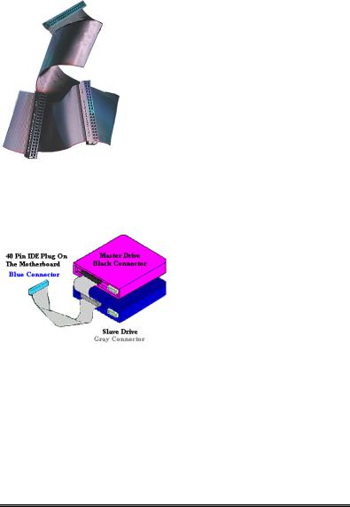
How to install the Ultra ATA/66 Cable Assembly:
& The BLUE connector MUST be plugged into the motherboard or your system will not work.
& Each connector on the Ultra ATA/66 cable assembly has a small polarization tab centrally located on the body of the plastic. This fits into the matching slot on the mating plugs on the motherboard and the drives,
thus assuring positive mating (pin #1 to pin
Figure 2-10. How to connect an ATA/66
#1)
Cable to the Motherboard
&The red line on the cable should be aligned with pin #1. On the drives this will result in the red line facing the power connector. Attach the BLUE connector to the appropriate 40 pin IDE plug on the motherboard.
&Attach the BLACK connector to the mating plug on the master hard drive. Attach the GREY connector to the mating plug on the slave drive (secondary hard drive, CD ROM, or tape drive). Please refer figure 2-10.
BE6
Installing the Motherboard |
2-17 |
|
|
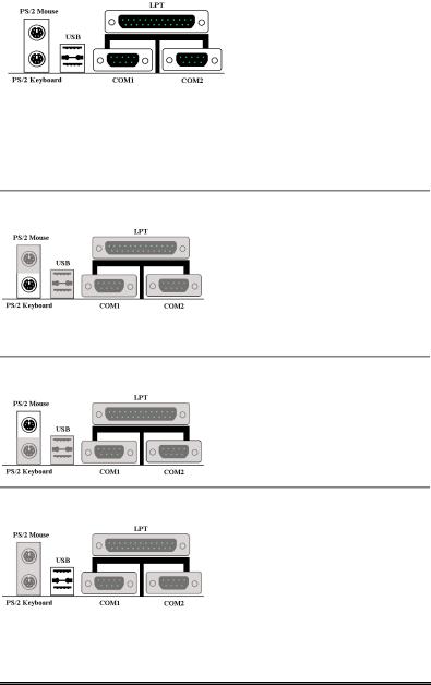
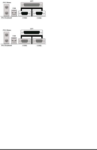
Figure 2-11. BE6 back panel connectors
Figure 2-11 shows the BE6 back panel connectors, these connectors are for connection to outside devices to the motherboard. We will describe which devices will attach to these connectors below.
KM1 Lower: PS/2 Keyboard Connector
Attach a PS/2 keyboard connector to this 6- pin Din-connector. If you use an AT keyboard, you can go to a computer store to purchase an AT to ATX converter adapter, then you can connect your AT keyboard to this connector. We suggest you use a PS/2 keyboard for best compatibility.
KM1 Upper: PS/2 Mouse Connector
Attach a PS/2 mouse to this 6-pin Dinconnector.
USB Port Connectors
This motherboard provides two USB ports. Attach the USB connector from the individual device to these connectors. You can attach USB devices such as a, scanner, monitor, mouse, keyboard, hub, CD-ROM, joystick etc. to one of each USB connector.
You must make sure your operating system supports this feature and you may need to install an additional driver for individual devices. Please refer to your device user’s manual for detailed information.
User’s Manual
2-18 |
Chapter2 |
|
|
|
|
Serial Port COM1 and COM2 Connector |
|
|
This motherboard provides two COM ports, |
|
you can connect an external modem, mouse |
|
or other devices that support this |
|
communication protocol. |
|
|
Parallel Port Connector |
|
|
This parallel port is also called an “LPT” |
|
port, because it usually connects to the |
|
printer. You can connect other devices that |
|
support this communication protocol, like a |
|
scanner, M.O. drive, etc. |
BE6

Introduction of the BIOS |
3-1 |
|
|
Chapter 3. Introduction of the BIOS
The BIOS is a program located on a Flash Memory chip on the motherboard. This program will not be lost when you turn the computer off. This program is also referred to as the boot program. It is the only channel for the hardware circuit to communicate with the operating system. Its main function is to manage the setup of the motherboard and interface cards parameters, including simple parameters such as time, date, hard disk drive, as well as more complex parameters such as hardware synchronization, device operating mode, CPU SOFT MENU™ II features and setup of CPU speed. The computer will operate normally, or will operate at its best, only if all these parameters are correctly configured through the BIOS.
'Don’t change the parameters inside the BIOS unless you fully understand their meanings and consequences
The parameters inside the BIOS are used to setup the hardware synchronization or the device operating mode. If the parameters are not correct, they will produce errors, the computer will crash, and sometimes you will even not be able to boot the computer after it has crashed. We recommend that you do not change the parameters inside the BIOS unless you are very familiar with them. If you are not able to boot your computer anymore, please refer to the section “Erase CMOS data” in Chapter 2.
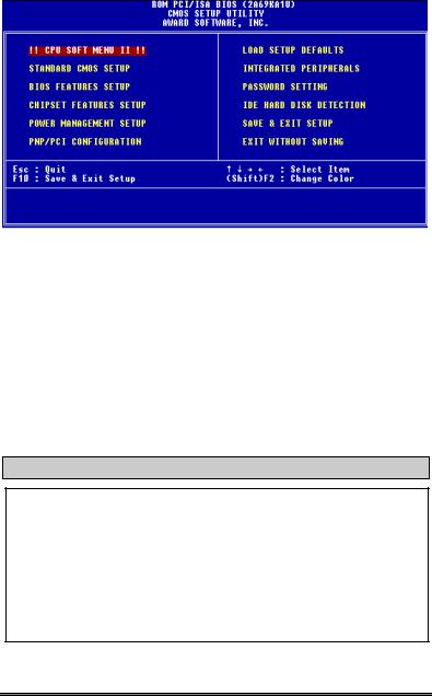
When you start the computer, it is controlled by the BIOS program. The BIOS first operates an auto-diagnostic test called POST (Power On Self Test) for all the necessary hardware, it then configures the parameters of the hardware synchronization, and detects all the hardware. Only when these tasks are completed does it give up control of the computer to the program of the next level, which is the operating system (OS). Since the BIOS is the only channel for hardware and software to communicate, it will be the key factor for system stability, and in insuring that your system performs at its best. After the BIOS has achieved the auto-diagnostic and auto-detection operations, it will display the following message:
PRESS DEL TO ENTER SETUP
The message will be displayed for three to five seconds, if you press the Del key, you will access the BIOS Setup menu. At that moment, the BIOS will display the following message:
User’s Manual
3-2 |
Chapter3 |
|
|
Figure 3-1. CMOS Setup Utility
In the BIOS Setup main menu of Figure 3-1, you can see several options. We will explain these options step by step in the following pages of this chapter, but let us first see a short description of the function keys you may use here:
!Press Esc to quit the BIOS Setup.
!Press ↑↓←→ (up, down, left, right) to choose, in the main menu, the option you want to confirm or to modify.
!Press F10 when you have completed the setup of BIOS parameters to save these parameters and to exit the BIOS Setup menu.
!Press Page Up/Page Down or +/- keys when you want to modify the BIOS parameters for the active option.
Computer Knowledge: CMOS Data
Maybe you have heard somebody saying that their CMOS DATA was lost. What is the CMOS? Is it important? The CMOS is the memory used to store the BIOS parameters that you have configured. This memory is passive. You can read its data, and you can also store data in it. But this memory has to be powered by a battery, in order to avoid any loss of its data when the computer is turned off. Since you may have to change the CMOS battery when it is out of power and if doing so, you will loose all CMOS data, therefore, we recommend that you write down all the parameters of your hardware, or to put a label with these parameters on your hard disk.
BE6
 Loading...